Formation energies of charged defects - manual workflow
Version: 2016.4
In this tutorial you will learn how to calculate formation energies of neutral and charged defects. Specifically, we will work with GaAs, which supports various charge states in both As and Ga vacancies.
You might also want to consult the introductory tutorial on formation energies, which focuses on bulk systems and neutral defects: Calculation of Formation Energies.
Note
In the O-2018.6 release, we introduced a so-called Study Object to automate the workflows described in this tutorial. That is now the recommended way of studying charged point defects in QuantumATK, and if you have access to O-2018.06 or newer, you should go to the corresponding tutorial Formation energies and transition levels of charged defects. Users of previous versions can still do the calculations and analysis using the more complex workflow, that is described here.

Procedure for calculating the formation energy
The formation energy \(E^f\) of a defect \(X\) is defined as the energy difference between the investigated system and the components in their reference states. This is analogous to the formation energy of a bulk material, but for charged defects it is less clear how to choose the reference states. Here we follow the procedure outlined in the review by C. Freysoldt et al. [1]:
\(E_{tot}[X^q]\) is the total energy of the defect state with charge \(q\), which is given in units of the elementary charge (\(e>0\)), \(E_{tot}[bulk]\) is the total energy of a bulk unit cell of the same size as the defected one, and \(n_i \mu_i\) is the reference energy of \(n_i\) added atoms of element \(i\) at chemical potential \(\mu_i\). The term in parenthesis accounts for the chemical potential of the electron(s) involved in charging the defect. \(E_{VBM}\) is the valence band maximum as given by the ATK band structure calculation for the bulk material of study (which is bulk undefected GaAs in this tutorial), and \(\mu_e\) is the electron chemical potential defined here with respect to the top of the corresponding valence band. The \(\mu_e\) parameter can then be treated as a free parameter, allowing to account for a shift of the Fermi level, e.g., due to doping. Note that \(\mu_e=E_{gap}/2\) corresponds to the undoped semiconductor case, where \(E_{gap}\) is the intrinsic semiconductor band gap. Finally, \(E_{corr}\) is a sum of relevant correctional terms. In our case, it corrects for electrostatic interactions between periodic images of the charged defects. Due to the long-ranged nature of the Coulomb interaction, it is very difficult to work with systems that are large enough not to need this correction. More details of the correction scheme can be found in the Appendix.
In order to calculate the formation energy, we need to compute each of the terms outlined above. The workflow is listed below:
Select the compound and defect to be investigated, and the computational model to be used (exchange-correlation, pseudopotentials, etc.).
Relax the pristine bulk system using the chosen computational model.
Determine the chemical potential of the elements in the defect. In this case we use the total energy of the bulk for the element removed to create the vacancy.
Setup the undefected supercell to calculate \(E_{tot}[bulk]\) and \(E_{VBM}\).
Introduce the (charged) defect and relax the system to obtain \(E_{tot}[X^q]\).
Calculate the correction terms in \(E_{corr}\) and finally the formation energy.
Neutral As vacancy in GaAs
As an example of a defect, we will calculate the formation energy of the As vacancy in GaAs, a vacancy which is capable of supporting many different charge states. However, we will first focus on the neutral vacancy defect, \(V^0\), before adding charge. In this case, the formation energy equation reduces to
The first two terms are straightforward to calculate, though possibly time-consuming. Conversely, the third term is the reference chemical potential for As, and our choice here has a direct impact on the absolute value of the computed formation energy for the defect. The most obvious choice here is bulk As, which is what we will use, but other choices may be sensible representations of specific situations. We will not go into details of the matter.
Total energies will be calculated using DFT with the PBESol exchange-correlation functional, a GGA-level approximation designed to work well for solids [2].
Optimized bulk geometry
We first need to relax the minimal unit cell and internal coordinates of the
GaAs and As bulks. For the latter, we also need the total energy per As atom.
Use a DFT calculator with PBESol and the  OptimizeGeometry object to relax the stress and forces on both bulks. This
is described in detail elsewhere, e.g. in the tutorial
Calculation of Formation Energies. For your convenience, we have also provided the
scripts here:
OptimizeGeometry object to relax the stress and forces on both bulks. This
is described in detail elsewhere, e.g. in the tutorial
Calculation of Formation Energies. For your convenience, we have also provided the
scripts here:
Larger supercell for bulk and defect calculations
Now find the optimized BulkConfiguration on the LabFloor, it should have an ID of gID001, and drop it on the Builder to set up a new BulkConfiguration with the optimized lattice constant. You may also find the optimized lattice parameter in the text output. However, we still need to make a bigger cell, and we would also like to have an orthogonal cell, as it will make the electrostatic corrections simpler.
To do this, select the GaAs system in the Stash and go to on the right, choose Conventional and click Transform. The GaAs is now represented by a, much larger, cubic cell.
We still need to make it bigger in order to get somewhat reasonable results for the defect, so go to and increase all three numbers to 2 and click Apply.
Now send this configuration to the Script Generator and add a New calculator, a Density of States object and a TotalEnergy analysis object.
Change exchange-correlation functional to PBES (for PBESol) and the k-point sampling to 4x4x4, which is adequate due to the large computational cell. Change k-points sampling in Density of States object to 8x8x8 k-points.
Now do the calculation - It should take about 10 minutes.
Warning
Please note that the 2x2x2 supercell used here is too small to get reliable (publication quality) results: The defect concentration is very high, and there will be (artificial) elastic interaction between the defects. At the end of this tutorial we will investigate how results change for a 3x3x3 cell.

Introducing a vacancy
To set up the neutral defect calculation you can either use the script
vacancy-calc.py or construct a script on your own. In the latter case, return to the
Builder and select the 2x2x2 orthogonal unit cell in the Stash. Then do the
following:
Select an As atom, preferably the one closest to the origin, and convert it to a ghost atom by clicking the
icon in the top bar.
Send this configuration to the Script generator and add a New Calculator, an OptimizeGeometry object and a TotalEnergy object.
Change the calculator settings to match those used for the pristine 2x2x2 GaAs. Default settings are fine for the other two objects. Run the calculation – it may take a couple of hours due to the geometry optimization.
Attention
Be aware that, in general, we need to account for the basis set superposition error, by leaving the basis functions associated with an atom when removing it to create the vacancy. In practice, this is achieved by making the atom into a ghost atom instead of removing it. This improves the result, perhaps only slightly, for most local basis sets, and carries an insignificant increase in computational cost.

Formation energy
We get total energies \(E_{tot}[GaAs]\) = -7460.13 eV for the defect-free bulk
configuration and \(E_{tot}[V^0]\) = -7285.59 eV for the configuration
with the neutral As vacancy, and combined with the result for the As bulk above, we
find a formation energy for the neutral As vacancy of 3.22 eV. You can also use the
script formation-energies.py to compute \(E^f[V^0]\).
Charged As vacancies in GaAs
Now that we have calculated the formation energy of the neutral defect, we turn our attention to incorporation of charges in our modeling. If we again focus on the As vacancy, the formation energy is computed according to:
The first term is similar to what we have just calculated for the neutral defect, while the second and third terms are exactly the same as previously and do not need to be re-calculated. The valence band maximum is determined through a density of states (DOS) calculation for the undefected bulk, while \(\mu_e\) will be treated as a free parameter. The last term, \(E_{corr}\) is calculated according to the scheme of Freysoldt et al. [3] , which also includes a small correction to the VBM, to account for the shift introduced by the defect, as discussed in the Appendix. Note that the correction term depends on the screening properties of the bulk material surrounding the charged defect. That requires knowing the dielectric constant value for the undefected bulk GaAs that can be either taken from experiment or computed as further explained in the Appendix.
Charged defects
The As vacancy can sustain a total of 5 charge states, including the neutral one considered above. We will now calculate the formation energies of these defects. For very large systems it may be worthwhile to use the relaxed state of the neutral defect as the initial guess for the charged ones, but this is not important for the system size used here.
The charges can either be added in the calculator when following the procedure
described above, or by directly making copies of the script and adding
charge=q, in the calculator object. You can also use the script vacancy-calc.py,
which will take the .nc file of a large bulk supercell as input and
add a defect before optimizing the geometry and computing the total energy.
Note
Remember to modified the entries defect_charge and saved_filename in the
input section of script vacancy-calc.py to select the correct charge state and the
name for the corresponding output file.
Formation energies
Now that we have all the pieces we need, we can calculate the full formation
energies by extracting the total energies from the saved data files and
calculating the correctional terms. For this, you can use the script formation-energies.py.
It takes as input the .nc files with the relaxed defect states, as
well as an undefected supercell of the same size including a valid DOS
calculation. You will also need the dielectric constant, calculated using your
chosen computational model, as detailed in this tutorial:
Optical Properties of Silicon. We also show how to do it for GaAs in the
Appendix.
Charge state |
Formation energy (with \(E_{corr}\) included) |
Periodic correction |
Band offset correction |
|---|---|---|---|
+1 |
3.04 eV |
0.13 eV |
-0.03 eV |
0 |
3.22 eV |
0.00 eV |
0.00 eV |
-1 |
3.56 eV |
0.13 eV |
0.00 eV |
-2 |
4.23 eV |
0.54 eV |
-0.03 eV |
-3 |
5.18 eV |
1.20 eV |
-0.10 eV |
The formation energies given above were calculated for an electron chemical potential at the VBM, that is, for \(\mu_e = 0\) eV. Considering \(\mu_e\) as a free parameter that shifts the Fermi level, we can also plot the formation energy for each defect as a function of the electron chemical potential. This would correspond to varying the doping level of the material. The effect is illustrated in the figure below, where the most stable charge state at a given \(\mu_e\) is identified with the lowest line. This shows that in p-type doped GaAs, corresponding to \(\mu_e = 0\) eV, the As vacancy is most stable with a positive charge. By increasing the electron chemical potential, the most stable charge state changes to neutral and from about \(\mu_e > 0.35\) eV, the most stable state is negatively charged. In particular, the As vacancy with the charge \(q=-2\) is the most stable defect in the intrinsic (undoped) GaAs for which \(\mu_e = E_{gap}/2\sim 0.75\) eV.
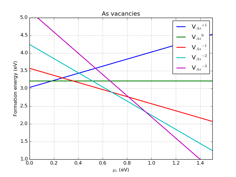
Fig. 104 Formation energy for various charge states of the As vacancy in GaAs as a function of \(\mu_e\) (defined with respect to the VBM), with the VBM at zero, computed with a 2x2x2 orthogonal supercell.
Influence of system size
If we increase the supercell size to 3x3x3, and change the k-point grid to 2x2x2, we find the formation energies listed in the table below, together with literature values from [4], which uses the same size of supercell.
Charge state |
2x2x2 |
3x3x3 |
Reference (3x3x3) |
|---|---|---|---|
+1 |
3.04 eV |
2.95 eV |
2.79 eV |
0 |
3.22 eV |
3.26 eV |
3.25 eV |
-1 |
3.56 eV |
3.67 eV |
3.33 eV |
-2 |
4.23 eV |
4.35 eV |
4.52 eV |
-3 |
5.18 eV |
5.25 eV |
5.86 eV |
We see how the formation energies are slightly different, with the shift being about 0.04 eV for the neutral defect. The difference is slightly larger for the charged defects, which is due to a slight shift of the VBM, caused by a slightly different k-point density. In this case there is not perfect agreement with the literature reference, but it should be noted that the reference does not use a ghost atom, and uses an older electrostatic correction scheme and LDA for exchange-correlation.
The changes also influence the plot of formation energy versus \(\mu_e\); although the slope of the lines are the same, their intercepts are slightly different, leading to a significant change in the overall picture of defect stability. Specifically, the neutral state is now only stable in a very narrow window, and the negatively charged states are most stable from \(\mu_e = 0.4\) eV.

Fig. 105 Formation energy for various charge states of the As vacancy in GaAs as a function of \(\mu_e\) (defined with respect to the VBM), with the VBM at zero, for a 3x3x3 orthogonal supercell.
Appendix
The periodic correction scheme
As already mentioned, we use the correction scheme proposed by Freysoldt et al. [3] to correct for the electrostatic interaction between the periodic images of the charges and the band shift caused by introduction of the defect. This correction contains two terms:
where \(E_{lat}\) corrects for the interaction between the periodic images of the charge and \(q \Delta V_{q/b}\) corrects for the band shift. \(E_{lat}\) is calculated by considering the electrostatics of a model charge distribution and comparing the potential in the periodic cell with the potential where the boundary conditions are not periodic:
\(V_q^{lr}\) is the long-range potential of the model charge distribution and \(\tilde{V}_q^{lr}\) is the corresponding quantity in the periodic cell. \(\Delta V_{q/b}\) is calculated from the shift in the electrostatic potential due to introduction of the defect:
where \(\tilde{V}_{q/b}\) is the difference between the electrostatic potential in the pristine bulk configuration and with the defect added. \(\Delta V_{q/b}\) should be evaluated far from the defect, where it is constant, in order to get the correct offset in the zero-point reference energy . In our implementation, it is averaged over the five grid points furthest from the defect. We plot these quantities in the figure below, where \(\Delta V_{q/b}\) is the black line:
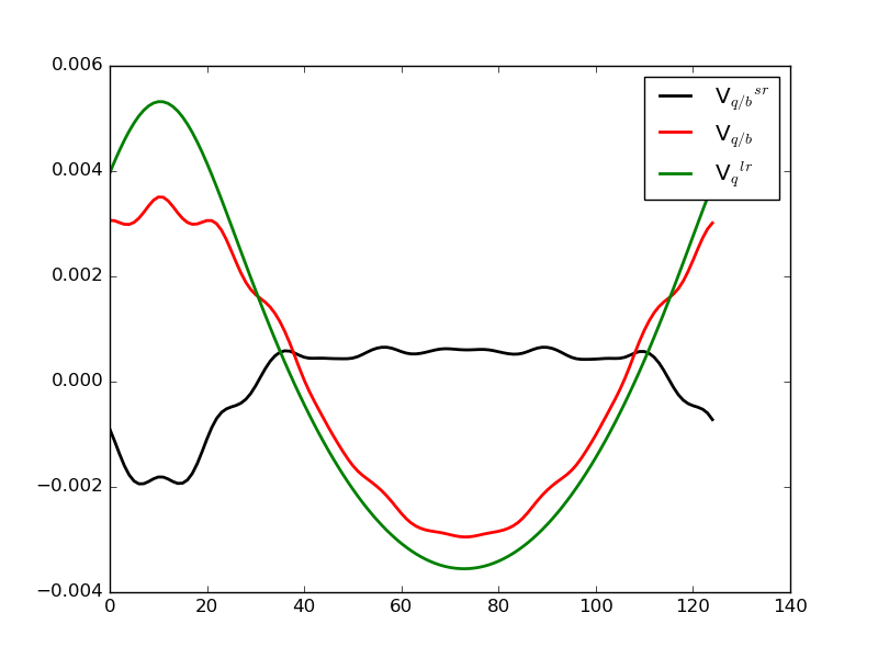
Fig. 106 Plot of the terms in the band offset correction. Green is the model potential from the defect, red is the change due to the introduction of the defect, and black is then the offset in the zero-point of the absolute energy.
Note that the obtained difference is defined between two screened potentials, see the reference [3] and the script formation-energies.py, where the screening is due to the semiconductor material surrounding the charged defect. The dielectric screening is described by the static dielectric constant computed in the following section for bulk GaAs.
Dielectric constant of GaAs
To account for the screening effect of the semiconductor material (surrounding the charged defect) on the band offset correction, one should compute the dielectric constant to be used in the script formation-energies.py. The dielectric constant can be calculated through an OpticalSpectrum analysis on a primitive GaAs bulk cell. It is important that the calculation is well-converged with respect to k-points, and also that the number of bands in the OpticalSpectrum is adequate for sampling all relevant transitions. In this case, a 20x20x20 k-point grid, 10 bands below the Fermi level and 20 bands above is sufficient to ensure this.
Drag and drop your optimized GaAs bulk structure to the Builder and send it to the Script Generator. Add a New Calculator and set it to the same parameters as the previous calculation, except for the k-points, which must be 20x20x20. Add an OpticalSpectrum analysis object, and set it to 20x20x20 k-points, 10 bands below the Fermi level and 20 above. The box should now look as the one in the figure below.

Run the calculation, which should take no more than a few minutes. You should now see the OpticalSpectrum on the LabFloor, which you can open with the Optical Spectrum Analyzer on the right. This will open a window with a plot which should look like this:

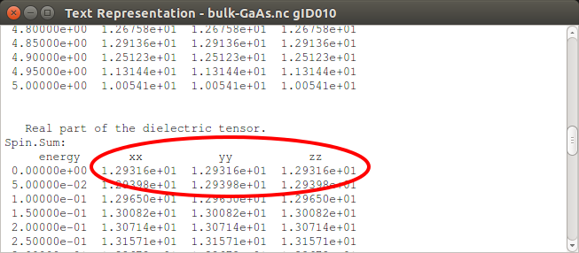
In this case, we are only interested in the intercept of the upper plot, which looks to be about 13. To get the exact calculated value, open the OpticalSpectrum with the Text Representation and find the part where it says “Real part of the dielectric tensor”. Here you can find the calculated value for the dielectric constant at zero frequency to be 12.9, as seen in the figure below:
References