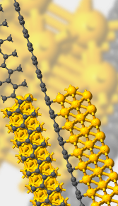
Graphene–Nickel interface
QuantumATK: Interface Platforms: Links: K. Stokbro et al., PRB 85, 165442 (2012) ATK can easily handle heterogeneous systems, where the two electrodes are not the same, as demonstrated in the above publication. Here you will learn how to build a similar system. |
|
Creating the structure
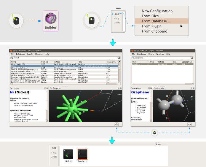
Step 1: Click . Locate nickel and add it to the Stash. Then also add graphene from the crystal database.
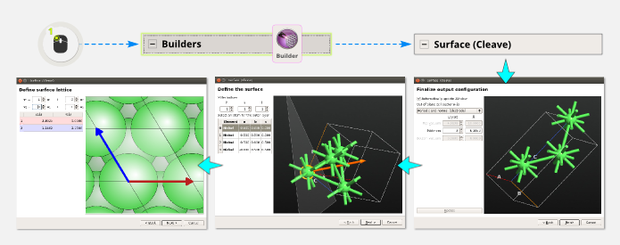
Step 2: Graphene fits very nicely onto Ni(111), so that’s the surface we’ll consider. Use the cleave tool to cleave the crystal along the (111) plane and make a 3-layer electrode cell.
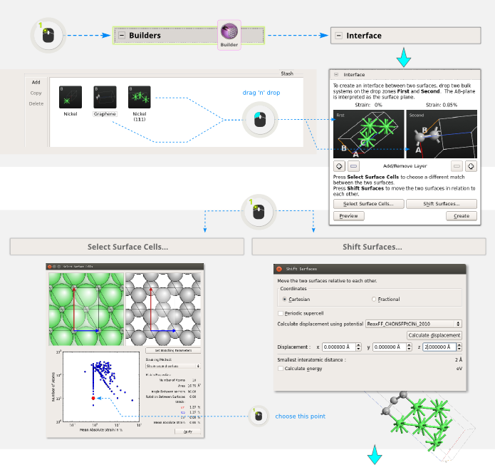
Step 3: Make an interface between the two system by opening . Drag the Ni(111) configuration to the first slot and graphene to the second slot.
Step 4: The suggested choice of cell is the minimal commensurate cell. This cell has hexagonal symmetry, but for this calculation it is more convenient to work with a rectangular cell. Therefore, click Select Surface Cells, and pick the cell with a slightly larger number of atoms but the same strain, as shown in the picture below. To choose this cell, click the corresponding point in the plot at the bottom left.
Step 5: Click Shift Surfaces and add 2 Angstroms to the Z position.
Tip
You can learn more about the Interface Builder in the Technical Notes on Interface Builder.
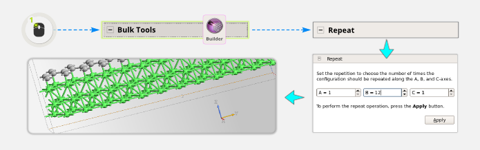
More configurations
Step 5: Use and repeat the structure 12 times in the B direction to make a larger sheet of graphene on an extended Ni(111) surface.
Step 6: Open and enter e=Ni and b>0.5. Press Enter or Tab, and then Delete. This cuts away half of the Ni slab.

Step 7: Decide how large a Ni–graphene interface you want, and then use the mouse to select and delete the superfluous carbon atoms.
Step 8: If you want to saturate the dangling bonds of the edge carbon atoms (cf. the article – you may or may not want to do this), select the edge atoms and use the passivation tool
 .
.Step 9: The system needs to be re-oriented, since the transport direction is always along Z. Use to swap B<->C, and Y<->Z (you should normally always swap twice to get a right-handed system).
Step 10: Finally, use to convert the structure to a device configuration; default option are fine so just click OK.