NEGF Simulations of Electron Transport in Devices
Version: Y-2026.03
In this tutorial, you will learn how to use QuantumATK NanoLab GUI to
Set-up and analyze electron transport simulations in the Si p-n junction device using the Non-equilibrium Green’s function (NEGF) method with the Semi-Empirical Tight-Binding model.
Analyze results, such as Hartree difference potential, projected local density of states (PLDOS), transmission spectrum and spectral current.
All the workflow, input and output files can be found in the Example Project - Y-2026.03 ‣ Si-p-n-device folder.
Prerequisites
Tutorial Geometry Optimization
Tutorial Band Structure, Projected Density of States and Effective Mass Calculations
Manual NEGF: Device Calculators

Building Si p-n Junction Device
Follow the tutorial Geometry Optimization to import the structure of bulk Silicon (alpha) from NanoLab’s Crystal Database to the
 Builder.
Create a Si(100) surface using the
Builder tool.Navigate to Builders ‣ Surface(Cleave) in the
Builder Panel (1).In the Surface(Cleave) window, choose the [1,0,0] Miller indices (2) and click Next (3).

Keep the 1×1 surface unit cell and click Next.
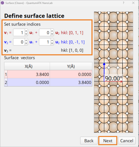
Select a thickness of 78 layers and click Finish.

Note
The 78 layers will constitute the central region of your device as explained in the NEGF manual NEGF: Device Calculators. You need such a relatively long device (~20 nm) because of the long screening length in the silicon semiconductor.
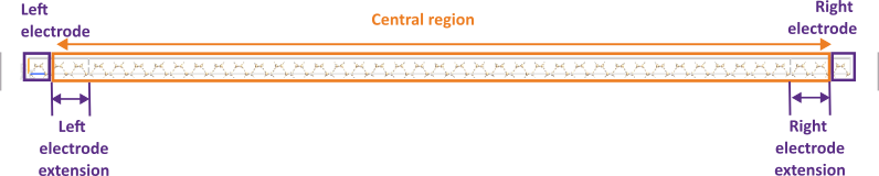
Construct a device with the transport direction along (100).
Navigate to Device Tools ‣ Device From Bulk in the
Builder Panel.Keep the default parameters for minimal electrode lengths and electrode extension lengths.
Click OK.
The created device configuration is automatically saved in the
Builder Stash and has the central region, left/right electrodes and lef/right electrode extensions.

Tip
When using a Semi-Empirical Tight-Binding models for NEGF electron transport, one can use the electrode extensions as small as possible, in particular for Nearest Neighbor models, such as Bassani.
When performing DFT-NEGF simulations, it is recommended to use longer electrode extensions. The required length will depend on the basis set and xc-functional. In particular when using hybrid DFT functionals - electrode extensions should be 2-3 times longer than for non-hybrid functionals.
QuantumATK will print a warning if the elecrode extension is too short.
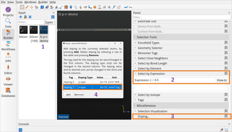
Set up p/n doping to have a Si p-n junction.
Highlight the device configuration in the
Builder Stash (1).Go to Selection Tools ‣ Select By Expression in the
Builder Panel (2).Type in c < 0.5 and press Enter to select all atoms in the left hand side of the device (2).
Go to Miscellaneous ‣ Doping in the
Builder Panel (3).Click Add to add doping for the left side, set the doping type (p-type) and the doping concentration (Value) of 2\(\cdot\)1019 cm-3 (4).
Follow the same procedure to select atoms with c > 0.5 to select all atoms in the right hand side of the device (2) and set the doping type (n-type) and doping concentration of 2\(\cdot\)1019 cm-3 to those atoms (4).
Setting up Electron Transport Simulations for the Si p-n Junction at 0 V Bias
You will use the Non-equilibrium Green’s function (NEGF) method NEGF: Device Calculators with Semi-Empirical Tight-Binding Bassani model parametrized for Si to calculate the ProjectedLocalDensityOfStates (PLDOS), HartreeDifferencePotential and TransmissionSpectrum for the p-n doped silicon junction at 0 bias. Calculating these properties will give you insights into the Si band gap on the p- and n-type sides of the device, band bending, depletion layer width and potential barrier at the p-n interface, left and right electrode chemical potentials and transmission spectrum, which can then be related to the current in the device.
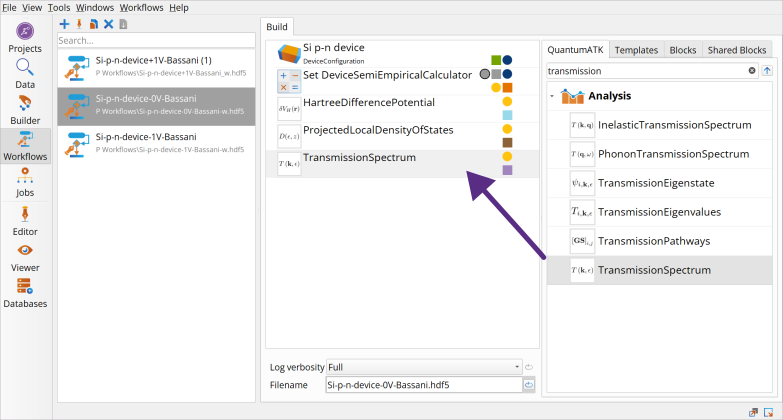
To create a workflow for electron transport NEGF calculations at 0 V bias in the  Workflow Builder, follow the step-by-step protocol described below.
Click on the
 Send content to other tools button to send the created device configuration from the Builder to the Workflow Builder.
Go to the Block Catalog ‣ QuantumATK tab ‣ Calculators category on the right hand panel and drag-and-drop the
 Set DeviceSemiEmpiricalCalculator block to the middle Workflow Area ‣ Build tab. Set the following parameters:
Use the default Slater-Koster Hamiltonian.
Leave the default Bassani.Si Parameter set
Uncheck No SCF Iteration box.
Use the default medium k-point density of 4 Å x 4 Å x 150 Å, which will result in a sampling of 7 x 7 x 174.
Under Poisson Solver, leave the default FFT2D Solver, which applies Periodic boundary conditions in A and B directions and open Dirichlet boundary conditions in the transport C direction.
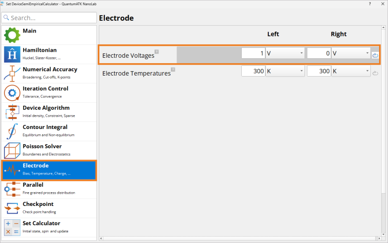
Under Electrode, leave the default 0V bias voltages and 300 K temperatures for electrodes.

Tip
Many k-points are needed in the transport (Z/C) direction in the electrode calculation to match the electronic structure of the electrodes and the central region. But it is relatively inexpensive since these k-points are only used in the electrode calculation, which is the smaller and faster part of the full computation.
Often you can use Semi-Empirical models in NEGF simulations, which are faster than DFT-NEGF, but DFT is more generally applicable and allows simulation of devices without the restriction of an available Semi-empirical model.
Go to the Block Catalog ‣ QuantumATK tab ‣ Analysis category on the right hand panel and drag-and-drop the following analysis object blocks to the middle Workflow Area ‣ Build tab.
HartreeDifferencePotential block
ProjectedLocalDensityOfStates block
TransmissionSpectrum block.
HartreeDifferencePotential has no adjustable parameters.
Edit the ProjectedLocalDensityOfStates block parameters:
For the Energies, increase the number of points from 200 to 401 in the -2.0 to +2.0 eV energy range for finer sampling.
For the k-point sampling, choose Density and click on Preset Densities to increase the k-point density from medium to high, i.e., 12 Å x 12 Å, which will result in a sampling of 20 x 20.
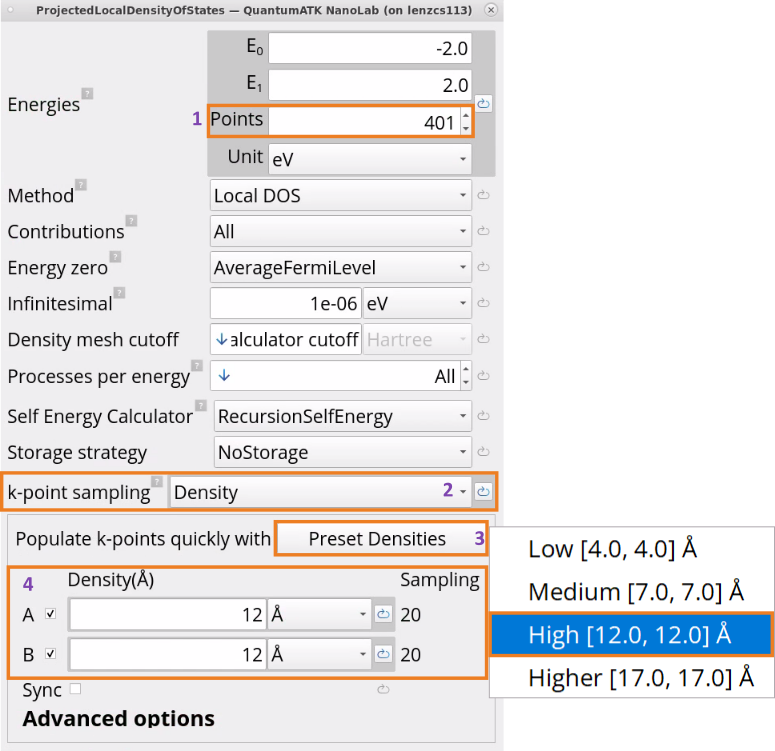
Edit the TransmisionSpectrum block paramaters:
For the Energies, choose Custom and increase the number of points from 200 to 401 in the -2.0 to +2.0 eV energy range for finer sampling.
For the k-point sampling, choose Density and click on Preset Densities to increase the k-point density from medium to high, i.e., 12 Å x 12 Å, which will result in a sampling of 20 x 20.

Note
It is important to have a large k-point sampling for electron transport properties, such as projected local density of states and transmission spectrum, as they depend on the conduction band minimum.
Change the Workflow name and Filename as needed (e.g., Si-p-n-device-0V-Bassani.hdf5)
Click on the
Send content to other tools button and choose Jobs as a script to send the workflow to the  Jobs tool to submit this job on a local machine or a remote cluster. Read these technical notes on Parallelization of QuantumATK calculations to learn how to best run NEGF simulations in parallel.
This also generates a Python script
Si-p-n-device-0V-Bassani.py, based on this workflow. It can be opened and edited with the Editor tool and then sent to the Jobs tool.
Analyzing Results at 0 V Bias
Once the calculation has finished, we are ready to analyze the results.
Go to the
 Data View tool.
In the Data Sources, select the file
Si-p-n-device-0V-Bassani.hdf5to see the list of calculated objects, HartreeDifferencePotential, ProjectedLocalDensityOfStates and TransmissionSpectrum in Data View.
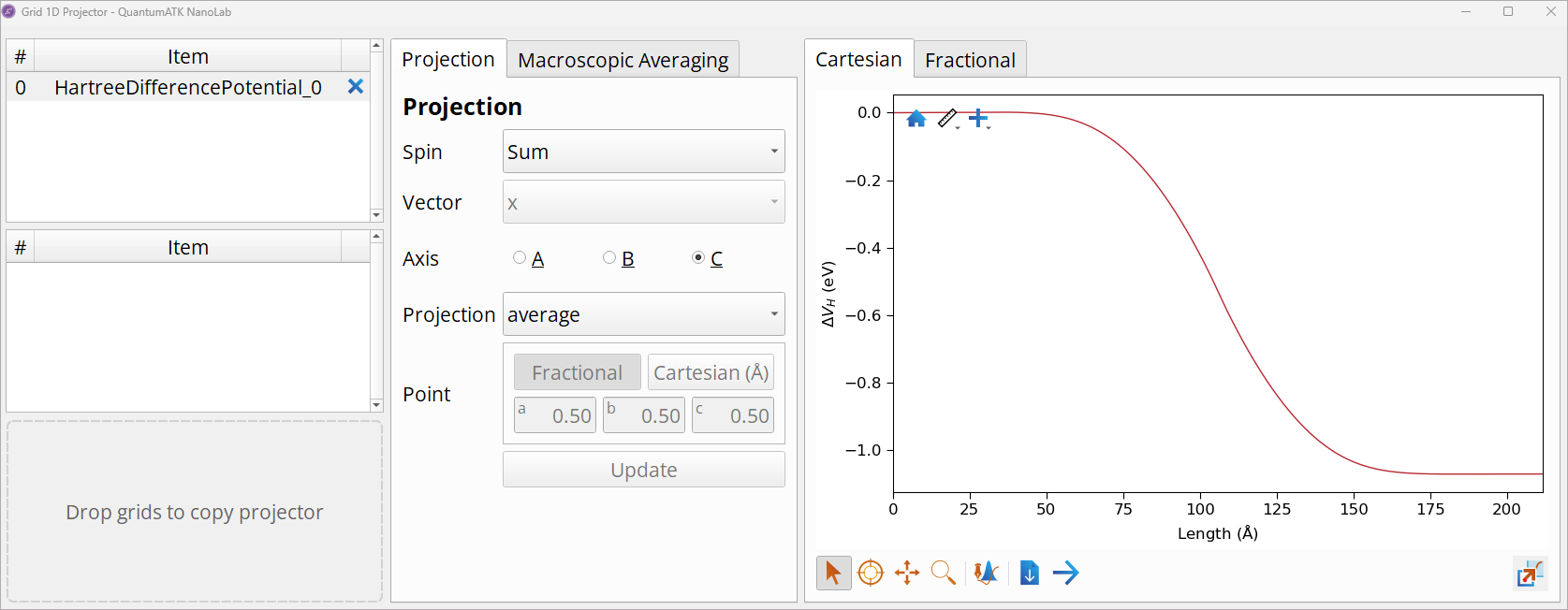
Double-click on the HartreeDifferencePotential to open it with the Grid 1D Projector and observe Hartree difference potential plotted along the device’s central region, which is ~20 nm long.
Note
The Hartree difference potential in the simulated Si p-n junction is flat towards the electrodes, indicating that the device is long enough, i.e., the number of Si layers in the left and right ends of the central region provide sufficient screening (the results are converged wrt. the length of the device). See the NEGF manual NEGF: Device Calculators for more info.
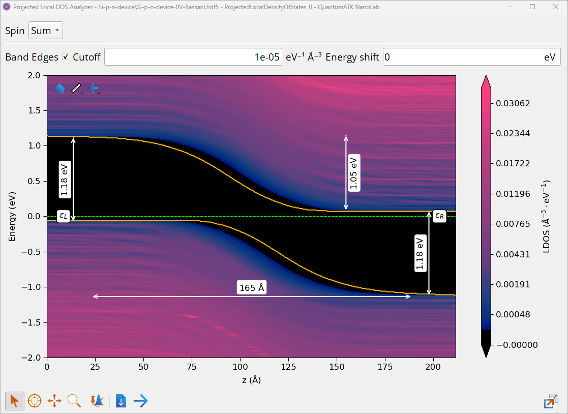
Double-click on the ProjectedLocalDensityOfStates object to open it with the Projected Local DOS Analyzer and investigate the projected local DOS of the Si p-n junction along the transport direction of the device.
Check the box Band Edges to visualize band edges.
Right-click to Add measurement ‣ Measure (vertical) or Add measurement ‣ Measure (horizontal) to measure a band gap, \(E_{g}\), along the device’s central region, depletion-layer width, \(W_{dep}\), and the built-in potential, \(\phi_{bi}\).
Note
Projected Local DOS shows that far from the p-n interface, we have a p-type semiconductor on the left side (with valence band maximum, \(E_{V}\), close to the Fermi level, \(ε_{L}\)) and the n-type semiconductor on the right side (with conduction band minimum, \(E_{C}\), close to the Fermi level, \(ε_{R}\)).
Measured Si band gap on the left (p-type) and right (n-type) sides of the device is ~ 1.18 eV, which is in a good agreement with the band gap calculated for bulk Si in Tutorial Band Structure, Projected Density of States and Effective Mass Calculations with the HSE06 hybrid DFT functional, GW [1] and experimental results [2]. This confirms that the Bassani tight-binding model parametrized for Si model gives reliable results in this case.
At the p-n interface (middle of the device) there is a depletion layer with \(W_{dep}\) ≃ 16.5 nm, where \(E_{C}\) and \(E_{V}\) are not flat (band bending) due to different doping types, resulting in the built-in potential across the junction (potential barrier at the junction), \(\phi_{bi}\) ≃ 1.05 eV, which opposes both the flow of holes and electrons across the junction.
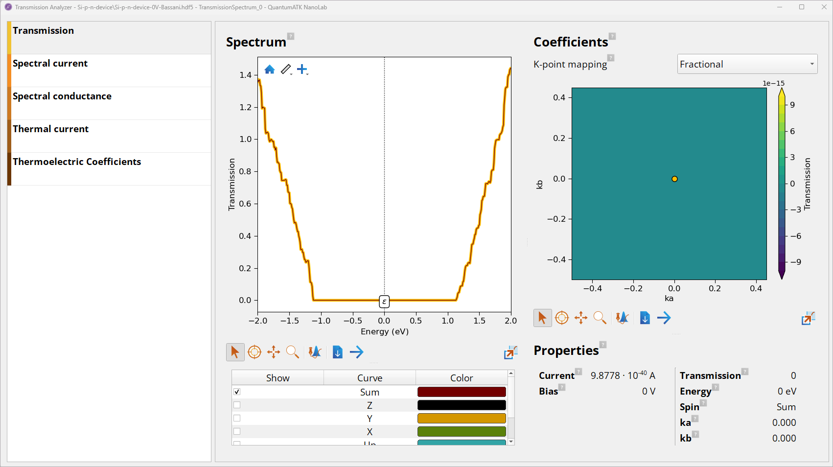
Double-click on the TransmissionSpectrum object to open it with the Transmission Analyzer to analyze transmission spectrum \(T(ε)\) at 0 V bias.
Note
The transmission \(T(ε)\) is zero in the band gap.
The electrical current \(I\) is calculated using the Landauer formula by intergating \(T\) across the energy range: \(I = 2e/h \int_{-∞}^{∞} dε T(ε)[f(ε-\mu_L)/(k_B T_L) - f(ε-\mu_R)/(k_B T_R)]\), where \(ε\) is electron energy and \(\mu_L\) and \(\mu_R\) are the left and right electrode chemical potentials, respectively. See the manual on TransmissionSpectrum to learn more.
At 0V bias the \(\mu_L = \mu_R = 0\), and so the current is 0.
You have just finished with analyzing Hartree difference potential, potential barrier, left and right electrode chemical potentials from the projected local density of states, and transmission spectrum for the Si p-n junction at 0 V bias. You will next perform the finite bias simulations to see the impact of the forward (+1 V) and reverse (-1 V) bias on the potential barrier, left and right electrode chemical potentials and transmission spectrum, which can then be related to the calculated current in the device.
Setting up Electron Transport Simulations for the Si p-n Junction at Finite Bias
To create a workflow for electron transport NEGF calculations at finite bias in the Workflow Builder, follow the step-by-step protocol described below.
To set up finite bias (\(V_{bias}\) = -1 and 1 V) simulations:
Go back to the
Workflow Builder.In the Workflow Stash, right-click on the 0 V bias workflow Si-p-n-device-0V-Bassani, choose Duplicate and do this twice.
Rename the two duplicates to Si-p-n-device-1V-Bassani for -1V and Si-p-n-device+1V-Bassani for +1V.
Double-click on the Set DeviceSemiEmpiricalCalculator block.
Under Electrode, change Electrode Voltages to -1V (left electrode) and 0 V (right electrode) to set up \(V_{bias}\) = -1 V.
Under Electrode, change Electrode Voltages to 1 V (left electrode) and 0 V (right electrode) to set up \(V_{bias}\) = +1 V.
Leave the rest of the settings unchanged.
Tip
When running finite bias calculations, there is a possibility to restart from 0 V bias or lower bias calculations to improve and speed-up the SCF convergence. To do this, use Load from file block in the workflow to set up from which calculation to restart and check Set with initial state box in the Set DeviceSemiEmpiricalCalculator block ‣ Set Calculator tab.
Analyzing Results at Finite Bias
Once the calculation has finished, we are ready to analyze the results.
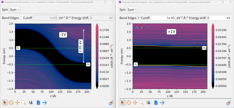
To analyze projected local density of states at finite bias (\(V_{bias}\) = -1, +1 V):
Go to the
Data View tool.In the Data Sources window, select a relevant hdf5 file (Si-p-n-device-1V-Bassani.hdf5 for -1V and Si-p-n-device+1V-Bassani.hdf5 for +1V).
In the Data View window, double-click on the ProjectedLocalDensityOfStates object to inspect the PLDOS plot for each bias value.
Right-click to Add measurement ‣ Measure (vertical) to measure the built-in potential, \(\phi_{bi}\).
Right-click to Add decoration ‣ Label to add labels.
Note
PLDOS at -1V (reverse bias) shows that \(ε_{L}\) = +0.5 eV and \(ε_{R}\) = -0.5 eV and the potential barrier is increased beyond \(\phi_{bi}\) by 1eV (2.05 eV in total).
PLDOS at +1 V (forward bias) shows that \(ε_{L}\) = -0.5 eV and \(ε_{R}\) = +0.5 eV and the potential barrier is decreased beyond \(\phi_{bi}\) by 1eV (to negligible ~ 0.05 eV in total).
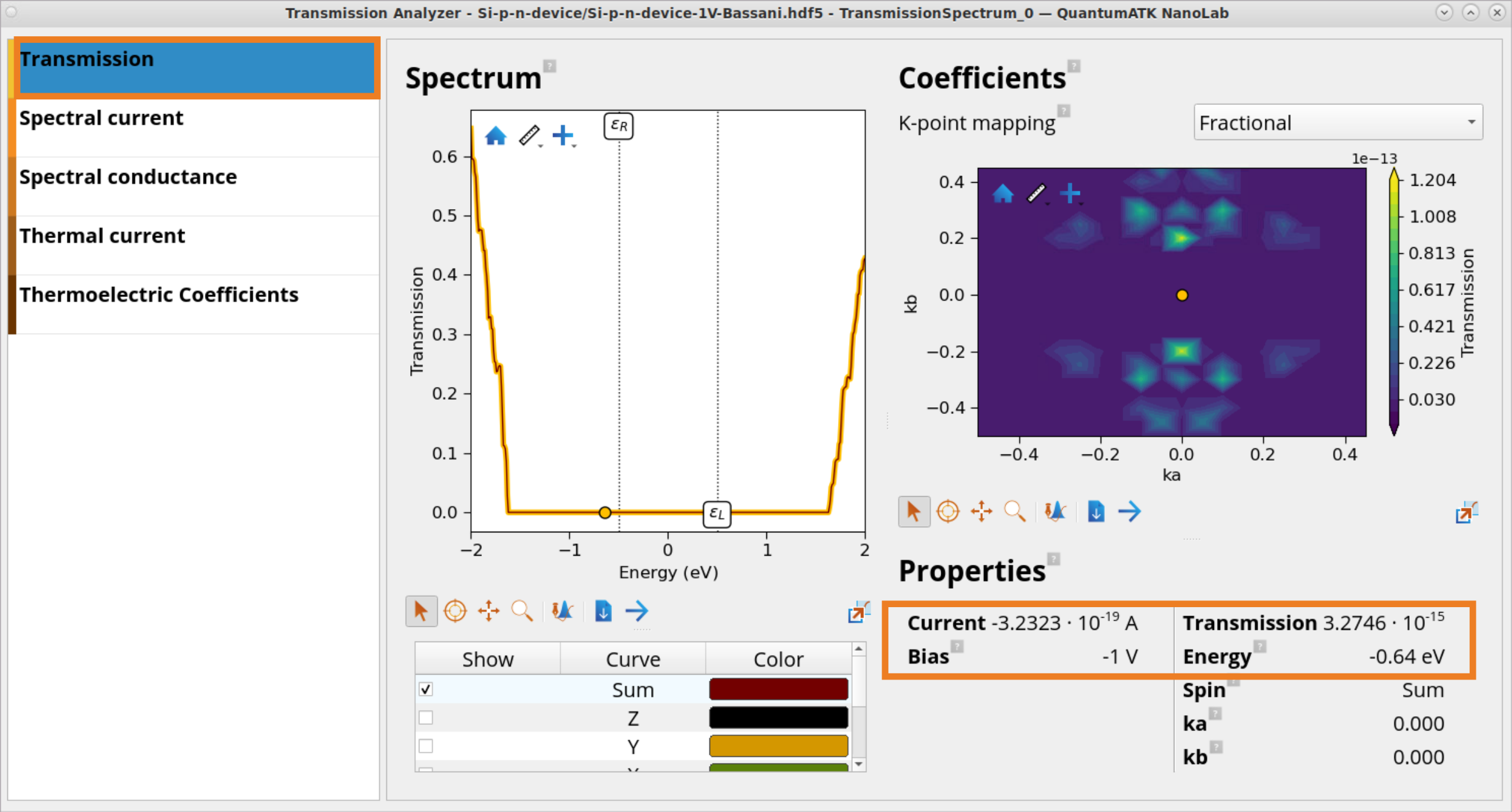
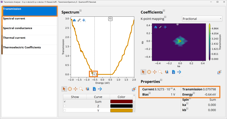
To analyze transmission spectrum at finite bias (\(V_{bias}\) = -1, +1 V):
In the Data Sources, select a relevant hdf5 file (Si-p-n-device-1V-Bassani.hdf5 for -1V and Si-p-n-device+1V-Bassani.hdf5 for +1V) and in Data View double-click on the TransmissionSpectrum object.
Click on the Transmission panel to inspect the transmission spectrum for each bias value. Spectrum window shows the transmission plotted as a function of energy, whereas Properties panel reports the total current and a transmission value at a chosen energy in the Spectrum plot.

Note
According to the Landauer formula shown above, electrical current \(I\) is calculated by intergating \(T\) across the energy range, and so the size of transmission has an impact on the observed current.
Under reverse -1 V bias, due to the increased potential barrier observed in the PLDOS plot, the transmission \(T\) around the bias window is close to 0 (e.g., 3.3 ⋅ \(10^{-15}\) at -0.64 eV) and so is the current, \(I\) = -3.23 ⋅ \(10^{-19}\) A.
Under forward +1 V bias, due to the decreased potential barrier observed in the PLDOS plot, the transmission \(T\) around the bias window is much higher (e.g., 0.08 at -0.64 eV and rapidly increases when going to larger energy values) and so the current is much larger: \(I\) = 8.9 ⋅ \(10^{-10}\) A.
This shows as expected, that the Si p-n device acts as a diode, which allows current to flow easily in one direction, but severely restricts current from flowing in the opposite direction.
Click on the Spectral current panel to investigate which energy states contribute most to the current, \(I\), at forward \(V_{bias}\) = +1 V bias, as the current depends not only on the size of transmission, but also available states that can transmit the current.
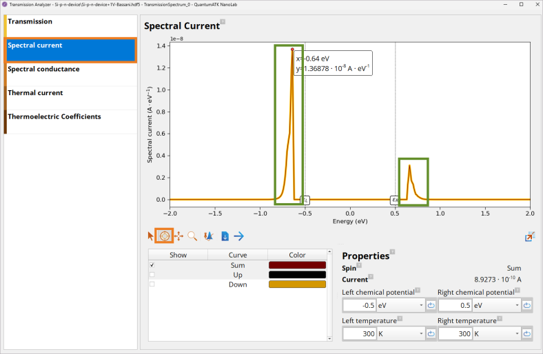

Note
Energy states at ~ -0.64 eV and 0.66 eV contribute most to the current, \(I\)
One can obtain TransmissionEigenstate and TransmissionEigenvalues by adding TransmissionEigenstate and TransmissionEigevalues blocks to the workflow.
It is also possible to vary the temperature of the Fermi-Dirac distribution in the left and right electrodes to see the temperature impact on the current, \(I\), in this case of an ideal structure. Note that this does not include electron-phonon coupling, which is beyond the scope of this tutorial.
Tip
Though there were no convergence issues in electron transport NEGF simulations of the Si p-n junction, sometimes one can encounter challenges in converging NEGF calculations to obtain the electronic ground state. In these cases, read the NEGF Convergence Guide which provides a list of action points for troubleshooting poorly converging NEGF calculations.
Summary and Outlook
In this tutorial, you have learnt how to set up and analyze projected local density of states, transmission spectrum and spectral current for a few bias points to demonstrate the principles of NEGF calculations of electron transport in devices. For more realistic studies, such as full \(I_d V_d\) and \(I_d V_g\) curves, we recommend to perform IVCharacteristics simulations. This is a combined framework for running multiple source-drain/gate voltage calculations and collecting and analyzing the results with “smart SCF restart“ functionality from lower bias simulations for faster and better SCF convergence.