Electrical characteristics of devices using the IVCharacteristics study object
Electrical characteristics of devices using the IVCharacteristics study object
Version: U-2022.12
This tutorial introduces the IVCharacteristicsstudy object used within
the framework of the Workflow Builder.
The IVCharacteristics study object enables the calculation and analysis
of the most relevant electrical characteristics of field-effect transistor (FET)
device models, including the on/off ratio (\(\mathrm{I_{on}/I_{off}}\)), the subthreshold slope
(\(\mathrm{SS}\)), the transconductance (\(\mathrm{g_{m}}\)) and the drain-induced barrier
lowering (\(\mathrm{DIBL}\)) [1].
In the present tutorial, you will learn how to use IVCharacteristics
study object in the Workflow Builder to setup, calculate and analyze some of the electrical
characteristics of a model silicon-on-insulator (SOI) device.
These workflows will be demonstrated for a preconstructed SOI FET device modeled with
the DeviceSemiEmpiricalCalculator adopted for the IVCharacteristics
study object to calculate the \(\mathrm{SS}\), and \(\mathrm{DIBL}\) parameter values and then benchmark
them against the available experimental data.
A general knowledge of the charge carrier transport in microelectronics devices and related IV characteristics is expected, e.g., IV curve, on/off ratio, subthreshold slope, transconductance, and drain-induced barrier lowering. If you are not familiar with these concepts you can still learn from this tutorial, but will not get the full benefit. If you wish to learn about them, we recommend reading this paper: [1].
Calculation and analysis of the \(\mathrm{I_{ds}-V_{gs}}\) curve for the FET on-state
The SOI FET device model structure considered in the tutorial is shown in the figure below. It consists of
a hydrogen-passivated 2D silicon slab, which includes a Si channel region connected with an ideal contact to source and drain leads made of highly-doped Si;
two continuum dielectric regions acting as the \(\mathrm{SiO_2}\) dielectric substrate or spacer (with \(\epsilon = 3.9 \epsilon_0\)) between a continuum metal gate
and atomistic Si channel region.
For the sake of computational efficiency, the electronic structure of the device model will be calculated
using a semi-empirical tight-binding model [2].
To create a workflow for IVCharacteristics calculations in the Workflow Builder, follow the step-by-step protocol described below. For a general introduction to the Workflow Builder, please see the dedicated guide: Introduction to the Workflow Builder.
To add the SOI FET device configuration (shown in the previous figure) to the NanoLab Builder, download the script soi_device_configuration.py, and drag-and-drop it on to the NanoLab Builder icon from the Data View. Or use the Add button in the NanoLab Builder to import the device structure from the script soi_device_configuration.py.
In the NanoLab Builder, send the SOI DeviceConfiguration to the Workflow Builder.
In the Workflow Builder window, add a Set SemiEmpiricalCalculator to the SOI Device workflow.
In the QuantumATK Search bar, type ivcharacteristics to find the corresponding IVCharacteristics study object and then add it to the workflow by double-clicking.
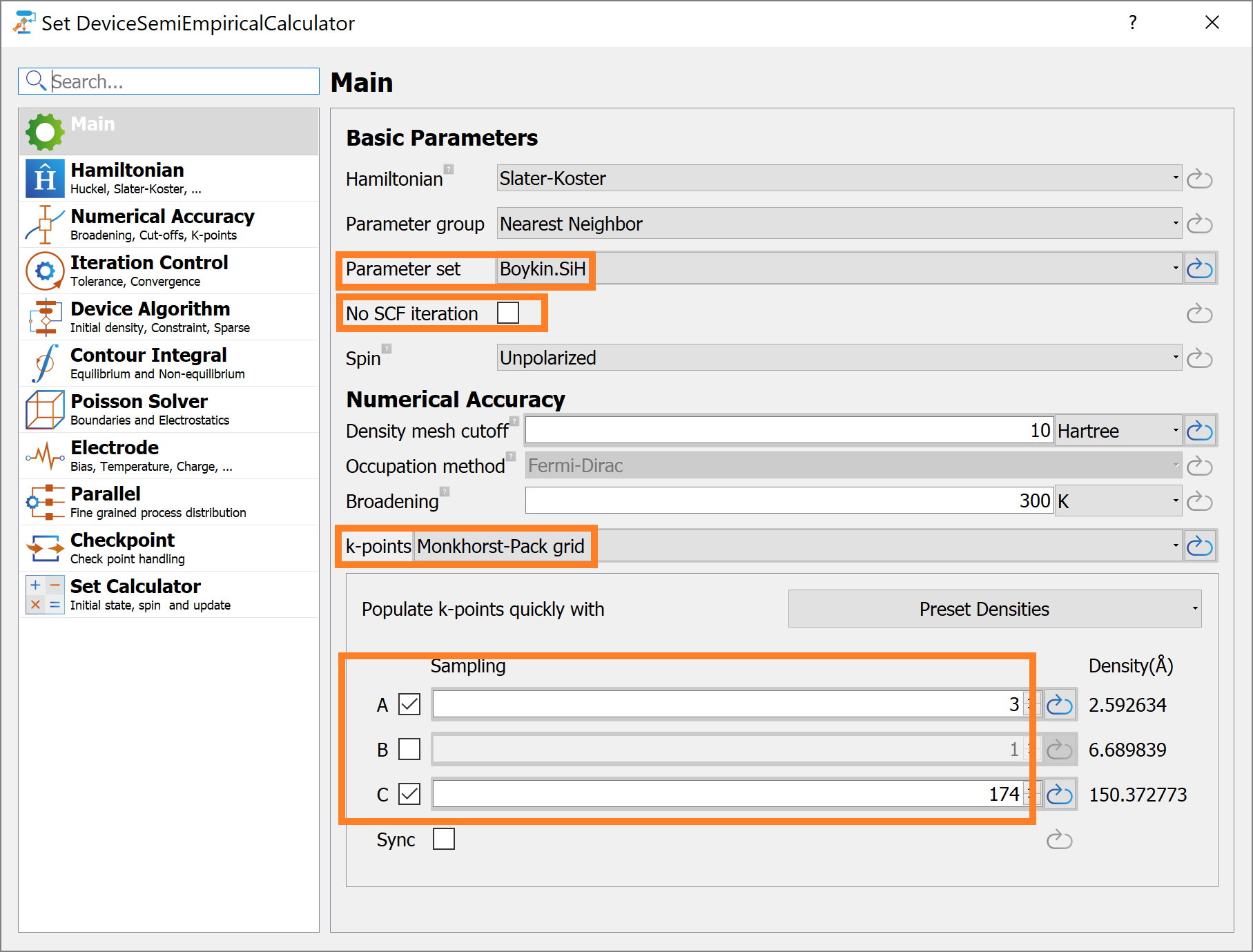
In the Main section of the Set SemiEmpiricalCalculator block, change the Parameter set to Boykin.SiH, uncheck the No SCF iteration box, change k-points from Density to Monkhorst-Pack k-grid, and set the k-point sampling to 3x1x174.
Change the Poisson Solver settings of the Set SemiEmpiricalCalculator block by switching to the [Parallel] Conjugate gradient Poisson solver, and set the top and bottom boundary conditions (in the B-direction) to Neumann, because there exists no periodicity in the direction perpendicular to the Si slab surfaces.
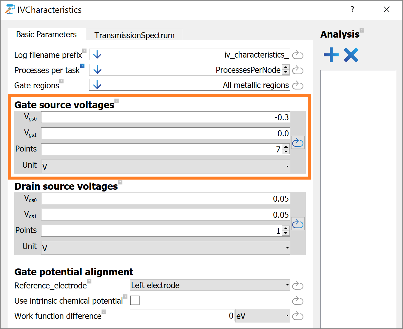
Edit the IVCharacteristics settings in the workflow to set a range of gate voltage values for calculating the \(\mathrm{I_{ds}}-\mathrm{V_{gs}}\) curve.
Note
Given these settings, the IVCharacteristics study object will do
a scan over the gate-source voltage values from \(\mathrm{V_{gs0}} = -0.3 \mathrm{V}\) to \(\mathrm{V_{gs1}} = 0.0 \mathrm{V}\),
at regular intervals of \(\mathrm{\Delta V_{gs}} = 0.05 \mathrm{V}\) and at a small drain-source bias voltage applied,
\(\mathrm{V_{ds}} = 0.05 \mathrm{V}\).
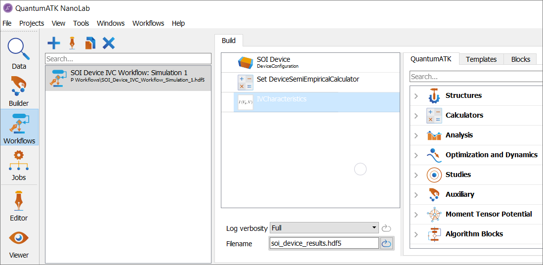
To verify if the SOI Device workflow in the previous section is created correctly, one can compare it to a predefined workflow, which can be downloaded at Workflow1. To use the predefined workflow, one should place the corresponding workflow (hdf5) file in your project folder in the Workflows subfolder (create it, if missing), and it will then appear in the Workflow Builder window of the QuantumATK NanoLab GUI as follows.
The SOI Device workflow created in the previous section and predefined SOI Device IVC Workflow: Simulation 1 are supposed to be identical. Rename the SOI Device workflow to SOI Device IVC Workflow: Simulation 1 in the Workflow Builder window.
To run the SOI Device IVC Workflow: Simulation 1, send it to the Job manager using the button, saving it, e.g., with a default filename ‘soi_device_results.py’. When submitting it to a Local Machine, then you might also need pressing the button in the Job manager to actually start running the calculation. This device calculation will take about 5 minutes using 40 MPI processes.
Once the device calculation is done (or started), go to the Data View (or to the working directory on a remote machine) and click on the log file soi_device_results.log in the Data View window (or use a text editor on the remote machine) to view the log information in the Editor. A list of all the planned tasks that are to be done by the IVCharacteristics study object can then be seen in the log, see the following figure with the first 3 (out of 14) workflow tasks highlighted in yellow.
 1+------------------------------------------------------------------------------+
 2| IV Characteristics Study                                                     |
 3+------------------------------------------------------------------------------+
 4| 14 task(s) will be executed.                                                 |
 5|                                                                              |
 6| * Update configuration                                                       |
 7|   Gate voltage: -0.3 V                                                       |
 8|   Left electrode voltage: 0.0 V                                              |
 9|   Right electrode voltage: 0.05 V                                            |
10| * Update configuration                                                       |
11|   Gate voltage: -0.25 V                                                      |
12|   Left electrode voltage: 0.0 V                                              |
13|   Right electrode voltage: 0.05 V                                            |
14| * Update configuration                                                       |
15|   Gate voltage: -0.2 V                                                       |
During the workflow execution, an additional information box will be printed out to the main log file for each started task of the workflow. In the following example of the main log file, there are 14 tasks to be executed, task 1 is finished and task 2 is in progress.
 1+------------------------------------------------------------------------------+
 2| Executing task 1 / 14:                                                       |
 3|   Update configuration                                                       |
 4|   Gate voltage: 0.0 V                                                        |
 5|   Left electrode voltage: 0.0 V                                              |
 6|   Right electrode voltage: 0.05 V                                            |
 7|   Log to: iv_characteristics_Vgs_0.0_Volt_Vds_0.05_Volt.log                  |
 8+------------------------------------------------------------------------------+
 9+------------------------------------------------------------------------------+
10| Executing task 2 / 14:                                                       |
11|   Calculate TransmissionSpectrum                                             |
12|   Gate voltage: 0.0 V                                                        |
13|   Left electrode voltage: 0.0 V                                              |
14|   Right electrode voltage: 0.05 V                                            |
15|   Log to: iv_characteristics_Vgs_0.0_Volt_Vds_0.05_Volt.log                  |
16+------------------------------------------------------------------------------+
Note
For each gate voltage point, the study object will create an additional log file with the usual NEGF-SCF convergence information, as well as information on related analysis object calculations, e.g., on the Transmission Spectrum calculation. We will not discuss that in more detail here.
Close the Editor and go back to the Data View of the QuantumATK NanoLab GUI. In the Data Sources, select the file soi_device_results.hdf5 and then click on (or right-click to Open with) the IVCharacteristics object in the Data View window to open the object, e.g., to view it with the IV-Characteristics Analyzer.
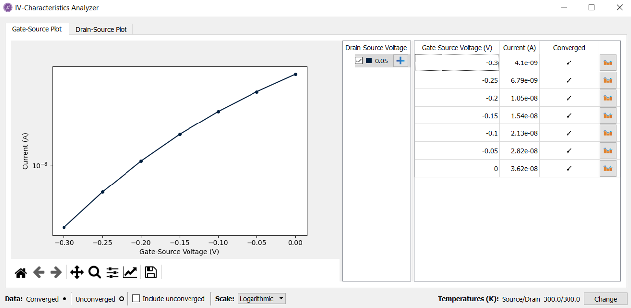
The IV-Characteristics Analyzer widget will then appear as follows.
The bottom part of the IV-Characteristics Analyzer widget contains the following supplemental information:
Data: the convergence information for individual self-consistent device calculations at different voltages. In this case all bias points are converged.
Note
An unconverged point in the \(\mathrm{I_{ds}}\ vs. \mathrm{V_{gs}}\) data set means that the NEGF-SCF calculation did not reach the target convergence parameter value (which is set in the Device Calculator) for the corresponding gate voltage value and are thus unreliable. For tips on how to reach the convergence target, see the guidelines in the NEGF Convergence Guide.
Scale: the plotting scale used on the Y-axis for the drain-source current \(\mathrm{I_{ds}}\), which can be viewed as either Linear or Logarithmic.
Temperatures: the electron temperature in the electrodes adopted to calculate the drain-source current \(\mathrm{I_{ds}}\), using the TransmissionSpectrum calculated by the IVCharacteristics study object. Note that the temperature for each electrode can be modified by the user, and the current is then re-calculated accordingly.
The top part of the IV-Characteristics Analyzer shows the actual plots of the IVCharacteristics data, allowing one to switch
between two different types of visualization:
Gate-Source Plot of the drain-source current vs. the gate-source voltage (\(\mathrm{I_{ds}}\ vs. \mathrm{V_{gs}}\) curve),
Drain-Source Plot of the drain-source current vs. the drain-source voltage (\(\mathrm{I_{ds}}\ vs. \mathrm{V_{ds}}\) curve).
Given that a single bias voltage \(\mathrm{V_{ds}}\) has been considered in this Workflow 1, only the \(\mathrm{I_{ds}}\ vs. \mathrm{V_{gs}}\) characteristics will be analyzed at this time.
To calculate relevant characteristics of the FET device, e.g., the subthreshold slope \(\mathrm{SS}\), click on the button in the Drain-Source Voltage section at the center of the panel and select the Subthreshold Slope option from the drop-down menu. The Gate voltage range over which the \(\mathrm{SS}\) is calculated will be highlighted in gray in the \(\mathrm{I_{ds}}\ vs. \mathrm{V_{gs}}\) plot. You can adjust this range to calculate the \(\mathrm{SS}\) in the Subthreshold Slope panel on the right-hand side of the screen.
Note
For the obtained \(\mathrm{I_{ds}}\ - \mathrm{V_{ds}}\) curve, the value of \(\mathrm{SS}\) is highly overestimated. The \(\mathrm{SS}\) value is also
very sensitive to the actual choice of the Gate voltage range. This is because the curve section, which is used to compute the \(\mathrm{SS}\) parameter here, lies outside the subthreshold region / FET off-state. In the latter, the current \(\mathrm{I_{ds}}\) is supposed to vary linearly (on a logarithmic scale) with \(\mathrm{V_{gs}}\).
For a reliable calculation of the \(\mathrm{SS}\), the range of \(\mathrm{V_{gs}}\) voltage values must therefore be extended
to the subthreshold region, or, in other words, to the FET off-state, as done in the following section.
Extending the range of the \(\mathrm{I_{ds}-V_{gs}}\) curve to the FET off-state
To sample the subthreshold region for the SOI FET device considered, the range of \(\mathrm{V_{gs}}\) has to be extended to
\(-0.9 \mathrm{V} \leq\ \mathrm{V_{gs}} \leq 0.0 \mathrm{V}\). This can be achieved in two ways:
2A. Extending the gate-source voltage range through the QuantumATK NanoLab GUI in the Workflow Builder
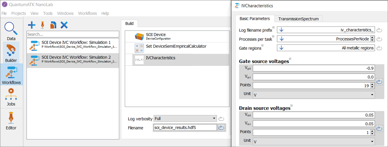
To extend the gate-source voltage range in the Workflow, one can select the SOI Device IVC Workflow: Simulation 1 (described in Section 1) and copy it with the Duplicate button, rename it to the SOI Device IVC Workflow: Simulation 2 in the Workflow Builder window to then modify the Gate source voltage range settings in the IVCharacteristics study object as follows:
Set the lower limit to \(\mathrm{V_{gs0}} = -0.9 \mathrm{V}\),
Set the number of voltage points to 19 to also include the original gate voltage range (for the on-state), \(-0.3 \mathrm{V} \leq\ \mathrm{V_{gs}} \leq 0.0 \mathrm{V}\), see also a note in the following.
Note
For the sake of comparison, the predefined SOI Device IVC Workflow: Simulation 2 is enclosed to this tutorial and can be downloaded at Workflow2.
To do the Workflow 2 for the extended gate voltage range, send SOI Device IVC Workflow: Simulation 2 to the Job manager using the button, save it as soi_device_results.py and press the button to run the corresponding job, if needed. The calculation will take about 5 minutes using 40 MPI processes.
Inspecting the log file of the follow-up Workflow 2 calculation, one can notice that only the \(\mathrm{V_{gs}}\) voltage points added to the original gate voltage range of Section 1 have been calculated. It means that the IVCharacteristics study object automatically performs a check of which values of \(\mathrm{V_{gs}}\) have been already considered, and run calculations only for the remaining values of \(\mathrm{V_{gs}}\).
It is important that:
The output / results (hdf5) file obtained in Section 1 is located in the same folder as the soi_device_results.py file,
And the new output / results (hdf5) file for the Workflow 2 calculation has the same filename as that used for the Workflow 1 calculation in Section 1. In the present example, keep the Results file filename as ‘soi_device_results.hdf5’.
Note
The range of the gate-source voltage values and number of voltage points have been chosen such that
the gate-source voltage values in the range of \(-0.3 \mathrm{V} \leq\ \mathrm{V_{gs}}\ \leq 0.0 \mathrm{V}\)
are the same as those used in the section Section 1. This ensures
that the study object will not repeat any calculation in that gate-source voltage range.
2B. Use scripting to add data points to the IVCharacteristics study object
There exists another option to instruct the IVCharacteristics study object to do calculations for additional values of \(\mathrm{V_{gs}}\). That can be done through Python scripting by adding the required voltage values by directly modifying the script, e.g., if the original workflow is missing or one cannot run the QuantumATK NanoLab GUI for some reason.
Note
An extensive list of all the commands available to interact with the IVCharacteristics study object is available in the IVCharacteristics entry of the reference manual.
To do this, click on (or right-click to open with) the script soi_device_results.py in the Data View window (or just open this script in some text editor) to open it the Editor. Add the line highlighted in yellow in the IVCharacteristics block.
To run the device calculation, send the script to the Job manager using the button, save it as soi_device_ivc_through_scripting.py, and press the button in the Job manager, if needed. The calculation will take about 5 minutes on 40 MPI processes. You can also download the full script at soi_device_ivc_through_scripting.py.
Note
In general, we recommend to save Workflows and use them in the Workflow Builder,
as described in Introduction to the Workflow Builder. This allows for a higher flexibility in adjusting simulation settings and
the simulation workflow itself, e.g., by adding new or removing old workflow steps through the QuantumATK NanoLab GUI
in a simpler manner than in a script.
Analysis of the \(\mathrm{I_{ds}-V_{gs}}\) curve in the subthreshold region
Once the device calculations are done, you are ready to analyze the characteristics of the device
and extract the subthreshold slope \(\mathrm{SS}\), using the appropriate set of data, which includes the subthreshold region / FET off-state.
Similarly to the discussion in Section 1, click on (or right-click to open with) the
IVCharacteristics object contained in the file soi_device_results.hdf5 present in the Data view window to
open the IV-Characteristics Analyzer widget.
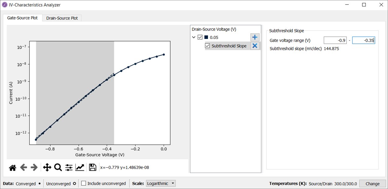
This time, the IV-Characteristics Analyzer will show an \(\mathrm{I_{ds}} - \mathrm{V_{gs}}\)
curve exhibiting a virtually linear behavior with respect to \(\mathrm{V_{gs}}\) in the gate voltage range of \(-0.9 \mathrm{V} \leq\ \mathrm{V_{gs}}\ \leq -0.35 \mathrm{V}\). This indicates that this range of \(\mathrm{V_{gs}}\) corresponds to the subthreshold region / FET off-state. Approximating the \(\mathrm{I_{ds}} - \mathrm{V_{gs}}\) curve with a linear fit allows for extracting the subthreshold slope \(\mathrm{SS}\).
Click on the button in the Drain-Source Voltage section at the center of the panel and select the
Subthreshold Slope option from the available options in the drop-down menu. Adjust the Gate voltage range in
the Subthreshold Slope panel to include only the subthreshold region by setting it from
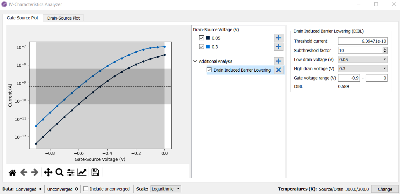
\(-0.9 \mathrm{V}\) to \(-0.35 \mathrm{V}\), as shown in the following figure.
The calculated value of the subthreshold slope is now \(\mathrm{SS} = 145\ \mathrm{meV/dec}\),
being of the same order of magnitude as a measured value of \(\mathrm{SS}^\mathrm{exp} = 95\ \mathrm{meV/dec}\)[3]. The discrepancy is related to a simplified model for the SOI FET device adopted in this tutorial for the sake of basic workflow demonstration.
To calculate the drain-induced barrier lowering (\(\mathrm{DIBL}\)), one needs to obtain a second \(\mathrm{I_{ds}}\ vs. \mathrm{V_{gs}}\) curve at a somewhat higher value of the source-drain bias voltage, \(\mathrm{V_{ds} = 0.3 V}\), for example.
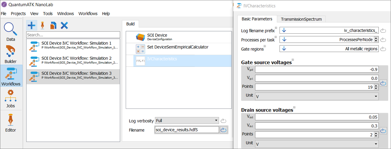
To extend the range of the source-drain voltage values in the study object, one can select the SOI Device IVC Workflow: Simulation 2 (described in Section 2A) and copy it with the Duplicate button, and rename it to the SOI Device IVC Workflow: Simulation 3 in the Workflow Builder window to then modify the Drain-source voltage range settings in the IVCharacteristics study object as follows:
Set the upper limit of the drain-source voltage range to \(\mathrm{V_{ds1}} = 0.3 \mathrm{V}\),
Set the number of points to 2.
Note
For the sake of comparison, the predefined SOI Device IVC Workflow: Simulation 3 is enclosed to this tutorial and can be downloaded at Workflow3.
To do the Workflow 3 for the extended gate voltage range, send SOI Device IVC Workflow: Simulation 3 to the Job manager using the button, save it as soi_device_results.py and press the button to run the corresponding job, if needed. The calculation will take about 10 minutes using 40 MPI processes.
It is important that:
The output / results (hdf5) file obtained in Section 2A is located in the same folder as the soi_device_results.py file,
And the new output / results (hdf5) file for the Workflow 2 calculation has the same filename as that used for the Workflow 1 calculation in Section 2A. In the present example, keep the Results file filename as ‘soi_device_results.hdf5’.
Note
By inspecting the log file, you will notice how, thanks to the smart handling of
pre-existing calculations, the IV Characteristics object has calculated only the curve at
\(\mathrm{V_{ds}} = 0.3 \mathrm{V}\), using the points calculated at
\(\mathrm{V_{ds}} = 0.05 \mathrm{V}\) as initial states until there are \(\mathrm{V_{ds}} = 0.3 \mathrm{V}\) points available.
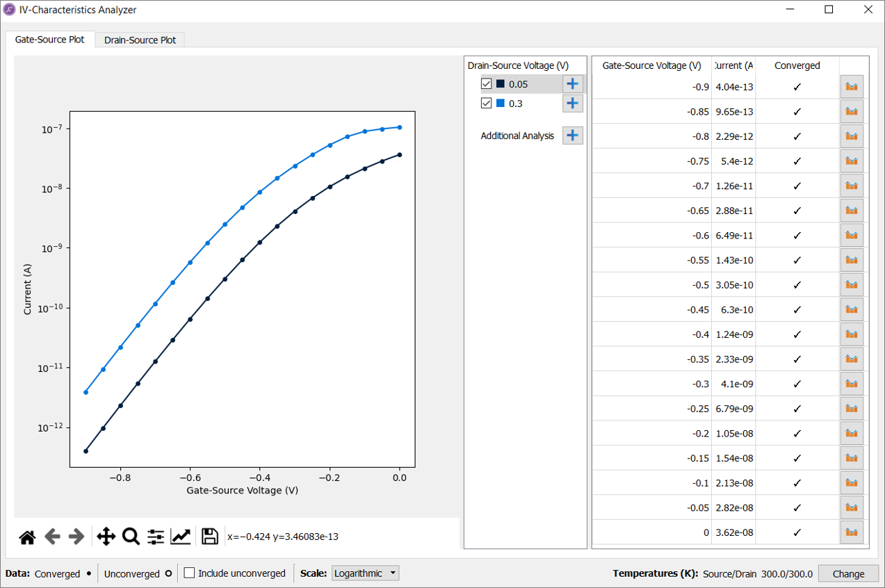
When the calculation is done, select the IVCharacteristics object contained in the file
soi_device_results.hdf5 in the Workflow Builder window, and click on the IV-Characteristics Analyzer plugin
in the right-hand side of the Quantum ATK NanoLab GUI window. The IV-Characteristics Analyzer plugin will now show also the
two additional curves calculated at \(\mathrm{V_{ds}} = 0.3 \mathrm{V}\), in addition to that previously calculated
at a lower bias voltage of \(\mathrm{V_{ds}} = 0.05 \mathrm{V}\), as shown in the following figure.
To calculate the \(\mathrm{DIBL}\) parameter, click on the button next to the Additional Analysis
option in the Drain-Source Voltage section at the center of the panel, and select
Drain Induced Barrier Lowering from the drop-down menu. The calculated value of \(\mathrm{DIBL}\)
will be shown in the Drain Induced Barrier Lowering section, as shown in the figure below.
Note
Notice that the \(\mathrm{DIBL}\) value of 0.589 is given as unitless quantity, which corresponds
to \(\mathrm{589\ mV/V}\) as often reported in literature.
There are a number of parameters that can be tuned in the Drain Induced Barrier Lowering panel
to tune the calculation of the \(\mathrm{DIBL}\). In particular, it is worth mentioning that:
The Threshold current, which is the value of the current corresponding to a value of \(\mathrm{V_{gs}}\) equal to the threshold voltage,
is set by default at the mid-point between the maximum and the minimum values of the current \(\mathrm{I_{ds}}\),
but can be modified by the user.
The Subthreshold factor determines the current range used to fit the subthreshold characteristics of
the device to accurately determine the threshold voltage. A range containing at least
3 points is then requested. If not enough points are included, the \(\mathrm{DIBL}\) will not be
calculated and an error message will be shown instead.
The Gate voltage range can be modified to include only that part of the curve for which the
\(\mathrm{DIBL}\) should be calculated. This can be important for device models showing
bipolar characteristics, where one has two subthreshold regions.
Warning
The value of the \(\mathrm{DIBL}\) calculated for the FET device considered in the present tutorial
is significantly larger than that measured experimentally. This can be ascribed to the high sensitivity of
the \(\mathrm{DIBL}\) parameter value to the doping profile and the geometrical characteristics of the device.
For a FET device with an ultra-short metal gate length, one can expect the \(\mathrm{DIBL}\) parameter value
between 0.1 and 1, as obtained in the present example.
 Workflow Builder.
The
Workflow Builder.
The 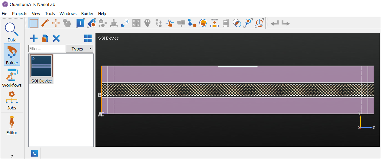
 NanoLab Builder, download the script
  Data View. Or use the
  Add button in the
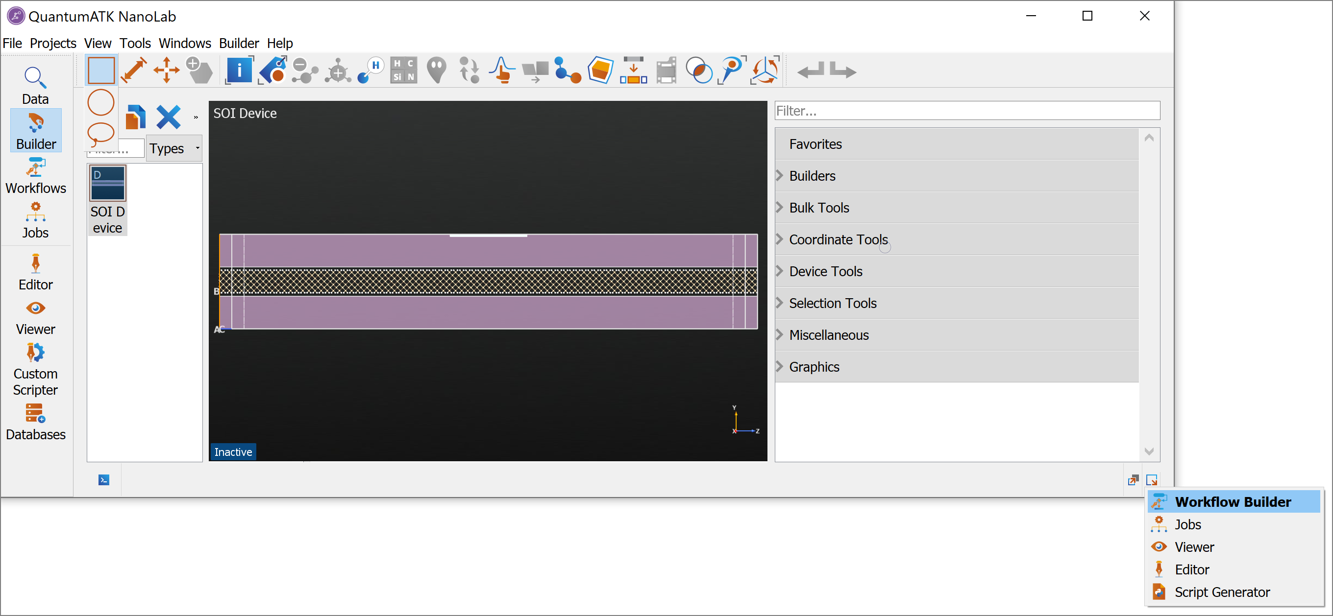
 Set SemiEmpiricalCalculator to the SOI Device workflow.
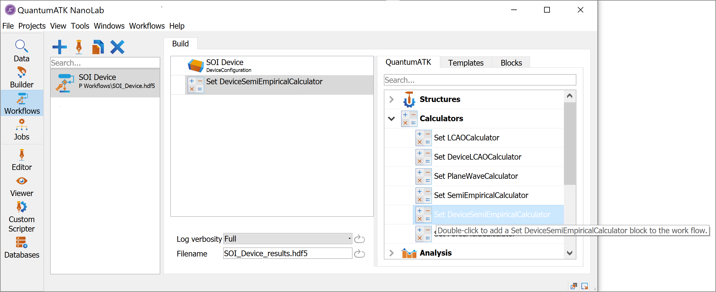
 IVCharacteristics study object and then add it to the workflow by double-clicking.
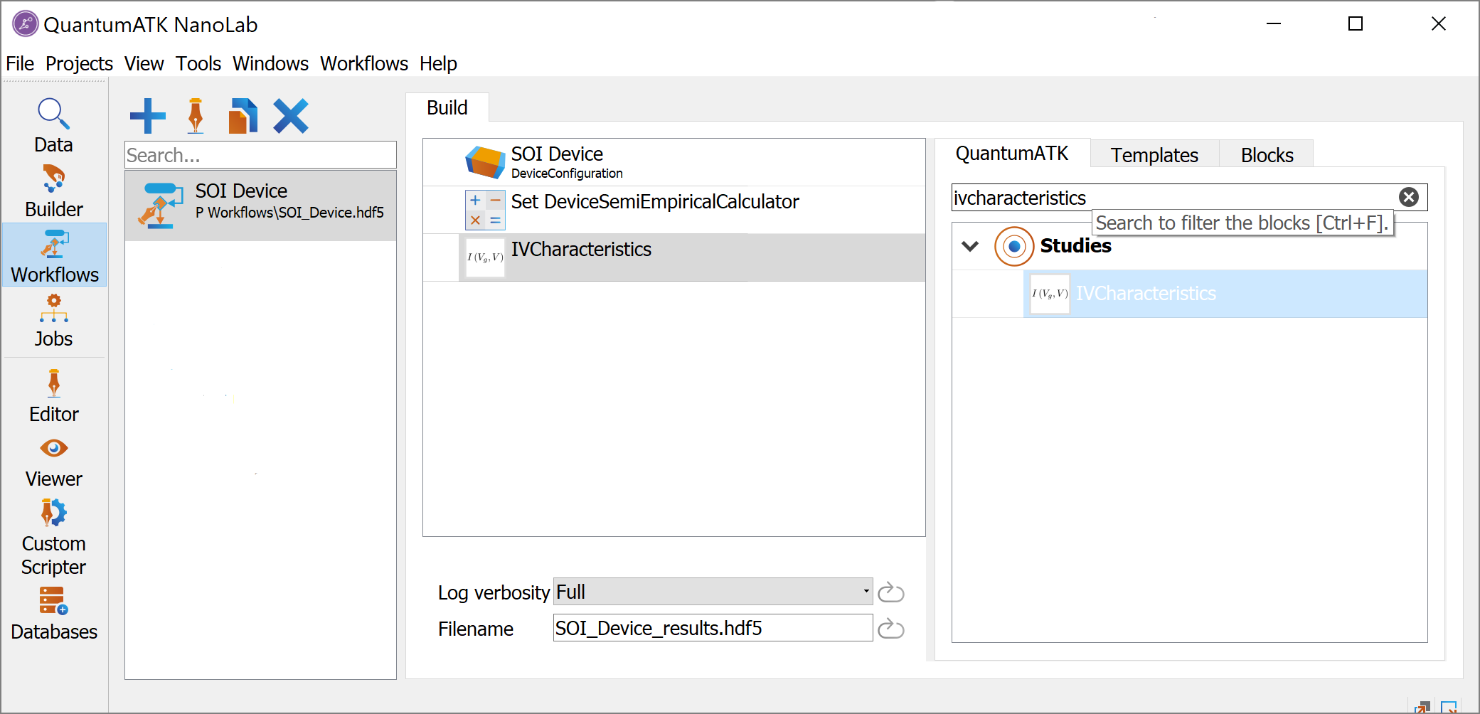
 Poisson Solver settings of the
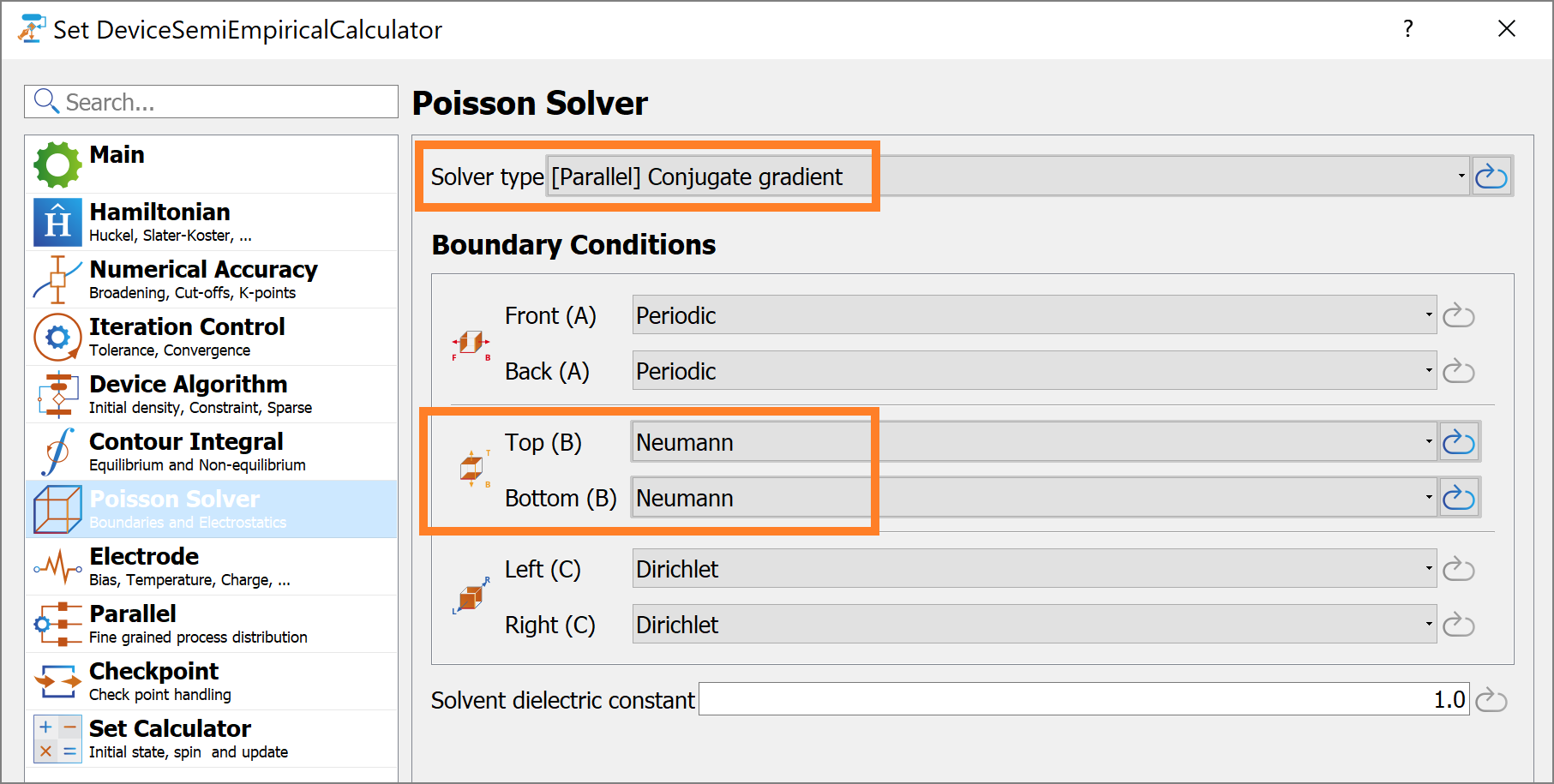
 Job manager using the
  button, saving it, e.g., with a default filename ‘soi_device_results.py’. When submitting it to a Local Machine, then you might also need pressing the
  button in the
  Editor. A list of all the planned tasks that are to be done by the
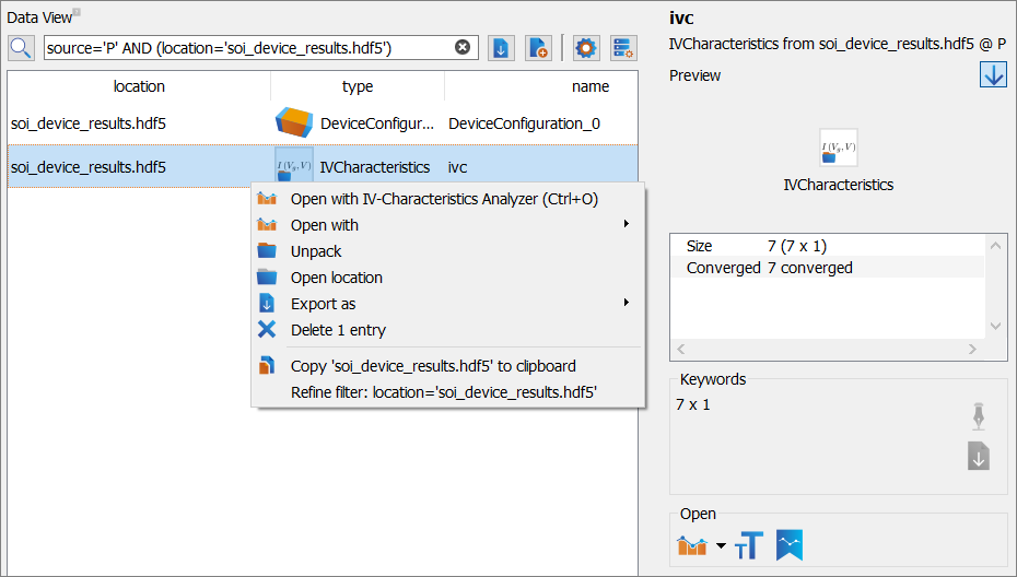
 button in the Drain-Source Voltage section at the center of the panel and select the Subthreshold Slope option from the drop-down menu. The Gate voltage range over which the \(\mathrm{SS}\) is calculated will be highlighted in gray in the \(\mathrm{I_{ds}}\ vs. \mathrm{V_{gs}}\) plot. You can adjust this range to calculate the \(\mathrm{SS}\) in the Subthreshold Slope panel on the right-hand side of the screen.
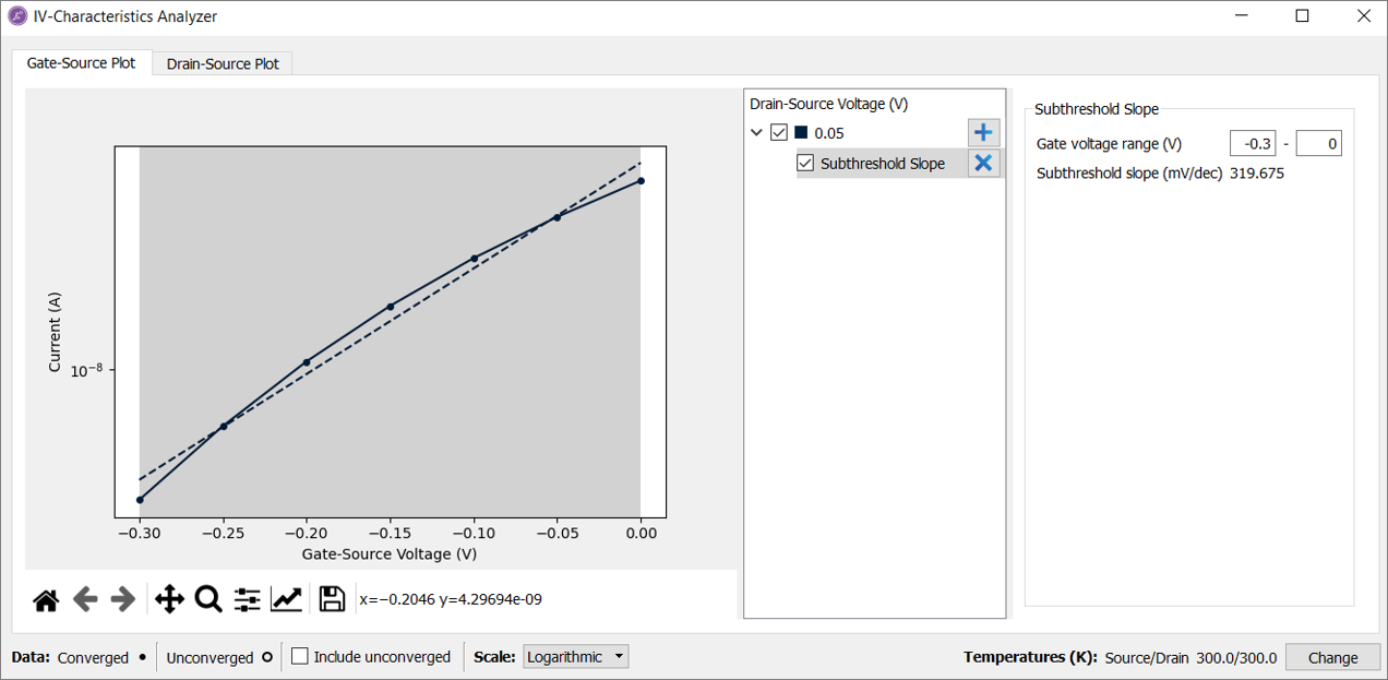
 Duplicate button, rename it to the SOI Device IVC Workflow: Simulation 2 in the