InAs p-i-n junction
Version: 2017
The purpose of this tutorial is to show how to set up and perform calculations for a device based on an InAs slab. You will define the structure of a H-passivated InAs slab along the (100) direction, and set up a p-i-n junction.
The underlying calculation engine for this tutorial is ATK-SE. A complete description of all the parameters, and in many cases a longer discussion about their physical relevance, can be found in the ATK-SE section of the ATK Reference Manual.
Tip
For more basic properties of InAs slabs, see this tutorial: Meta-GGA and 2D confined InAs

Setting up the device geometry
Creating a passivated InAs slab
Start QuantumATK and launch the Builder by pressing the  icon on the toolbar.
In the builder, click .
Type “InAs” in the search field and double-click on the row with InAs.
Click the
 icon in the lower right-hand corner of the Database window to add the structure to the Stash in the Builder.
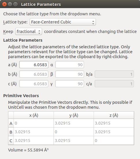
The next step is to change the lattice constant to the experimental room temperature lattice constant, a = 6.0583 Å [1].
In the panel to the right open .
Set Keep fractional coordinates.
Set a = 6.0583 Å.
We now have a bulk configuration with the correct lattice parameter, and the next step is to create a slab with the right orientation. Open to cleave the crystal. In this case, along the (100) direction.
Keep the default (100) cleave direction, and press Next >.
Keep the default surface lattice, and press Next >.
Keep the default settings on the last page, and press the Finish button to add the cleaved structure to the Stash.
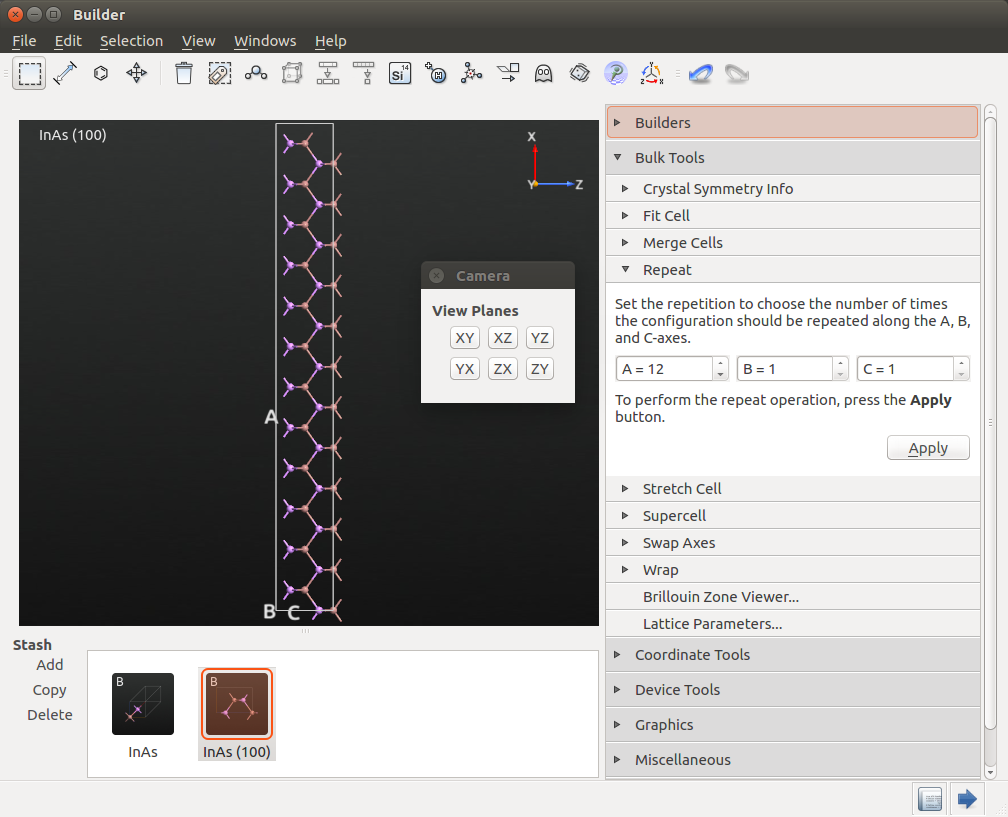
Open and enter A = 12, B = 1, and C = 1, and press Apply.
To get a good look at the structure, click on the viewplane icon  and choose ZX. You should now see the following:
At this point you should register the volume of this InAs cell. Open . The volume is printed in the Lattice Parameters window: 1334.15 Å3. You will need this value in the next section when we set up the doping of the p-i-n device.
To finalize the setup, perform the following steps:
Open . Select Keep Cartesian, and set the length of the A vector to 80 Å.
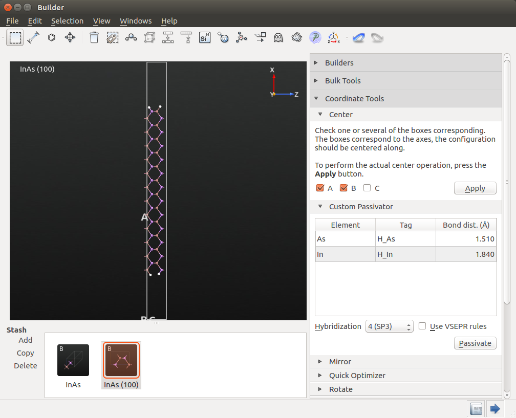
Open and center the structure in the A and B directions.
Open . Select Hybridization 4(SP3), and passivate the structure.
Your structure should now resemble the one shown below.
Warning
In previous versions of QuantumATK (2016 and earlier), we have identified a bug which caused some of the H atoms to miss their tags in some cases. If you use a version where this bug might apply, please check the tags of the H atoms, and manually apply the correct tag to any that are missing. We need these tags later when applying compensation charges and doping.
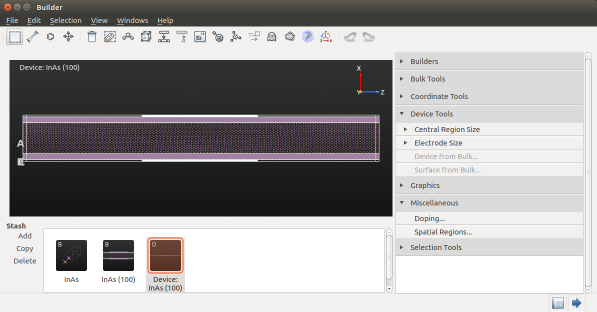
Creating the FET device geometry from the slab
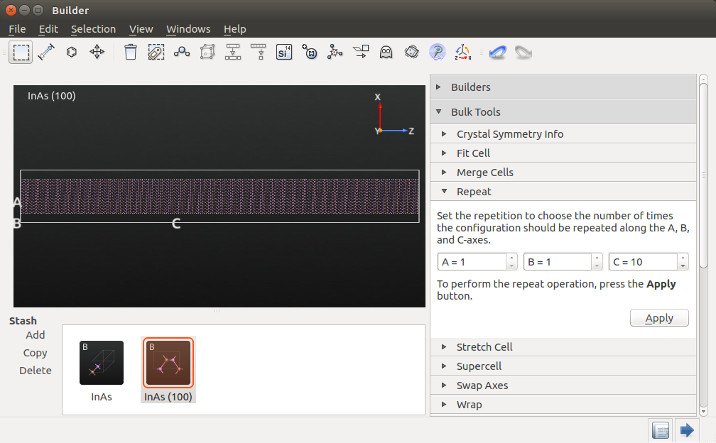
We will make a 60 nm long device, thus the unit cell must be repeated 100 times along C. Therefore, open the panel, set A = 1, B = 1 and C = 10, and press Apply twice. Your structure should now look like this:
Warning
The repeat panel remembers your settings from last time, so remember to change the value for A back to 1. If you forgot this, you can use the undo button  .
.
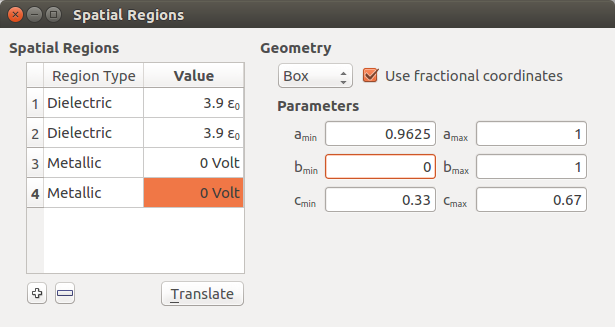
Adding dielectric regions and gates
The next step is to add 1 nm thick dielectric regions on both sides of the device with a double gate in the center.
Open .
Right-click in the white area of the widget and click Insert region to insert a new spatial region. You can also click on the
icon below the white area.Change the spatial region into a dielectric region and set the dielectric constant to 3.9. Define in fractional coordinates:
a: 0.0375–0.165,
b: 0–1,
c: 0–1.
Add another dielectric region with dielectric constant 3.9. Define in fractional coordinates:
a: 0.8375–0.9625
b: 0–1
c: 0–1.
Add a metallic region with value 0.0 Volt. Define in fractional coordinates:
a: 0–0.0375
b: 0–1
c :0.33–0.67.
Add another metallic region with value 0.0 Volt. Define in fractional coordinates:
a: 0.9625–1,
b: 0–1
c: 0.33–0.67.
Note
Note that you can switch between fractional and cartesian coordinates, if you prefer a particular representation of coordinates.
At the end, the widget should look like this, and you can close it:
Finally, transform the structure into a device configuration by opening . Accept the default suggestion for the electrode lengths of \(a\) = 6.0583 Å. The dielectric regions are automatically extended to the electrodes as well.
Warning
In previous versions of QuantumATK (2016 and earlier), this extension was not done automatically. If you use an older version, you can add the dielectric regions to the electrodes in the script, by inserting the contents of this file somewhere after the two electrodes have been defined: dielectric-regions.py
Adding doping to the configuration
Finally, we add the doping to the configuration, which includes both regions of In and As atoms, as well the passivating hydrogen atoms. As InAs is a III-V material, the passivating hydrogens should have fractional charges, as explained in this tutorial: Meta-GGA and 2D confined InAs.
Note
The doping can also be applied via a script. Send the device configuration to the  Editor, and append the contents of this script at the end:
 add-doping.py. You have now created the device, and are ready to set up the actual calculations.
Adding fractional charges to the H atoms
To add the correct fractional charges to the H atoms, go to the panel on the right, and select .
Click on H_As, which will select the H atoms bonded to As atoms.
Open , click Add, change the Unit to e/atom and the Doping Type to p-type.
Double-click on the number under Value and type 0.25 to apply a fractional charge of -0.25 electron to these H atoms.
Now, go back to and select H_In. Repeat the process above, but choose n-type to apply a charge of +0.25 electron instead. The doping widget should now look like this:
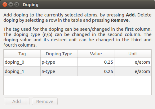
Tip
When using the doping widget, QuantumATK automatically assigns a tag to each atom, and you can easily edit these tags to make them more meaningful for your application.
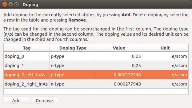
Adding p-type and n-type doping to InAs
Secondly, we dope the InAs with p-type doping at one end and n-type at the other, with an intrinsic region in the middle. Here, we will also use the doping widget, which can handily apply a doping with a specific volume concentration. However, because we already have vacuum in the configuration, we cannot use this feature, as it would be based on a too large volume. We would like a doping concentration of \(10^{19}\) per cm3, and with the 48 atoms and 1334.15 Å3 volume of the un-repeated slab, this works out to a doping value of 0.0002779479 e/atom, irrespective of the vacuum.
First, we will apply the p-type doping to the left side of the device. We will use the gate to define the intrinsic region, so zoom in on the left side of the device so that you can still see the whole electrode and the edge of the gate.
Tip
If you hold down the shift key and the right mouse button at the same time, you can move the configuration around the window. This is very useful in this case. See also the Mouse and key operations section of the Builder Manual.
Now select all the In and As atoms to the left of the gate, while not hitting any H atoms. Open the doping widget again, and apply a p-type doping of 0.0002779479 e/atom. Do the same to the right of the gate, but instead selecting n-type here. The doping widget should now look like this:
The device is now finished, and you are ready to begin calculations. You can download the full geometry here: full-device.py.
Running the calculations
Send the updated script from the Editor to the Script Generator.
Add a
 New Calculator
Select the ATK-SE: Slater-Koster calculator
Set the k-point sampling to 1, 11, 100 and uncheck the No SCF iteration box.
Iteration control parameters: set the number of history steps to 10. This will slightly improve the convergence for this system and it will reduce the memory consumption.
Device algorithm parameters: Set the Self energy method to Sparse Recursion for calculating both equilibrium and non-equilibrium contour integrals.
Poisson Solver: Select the [Parallel] Conjugate Gradient method and Neumann boundary conditions in the A-direction, where the gates are located.
Slater-Koster basis set: Select the Bassani.InAsH basis set.
Add an
 ElectrostaticDifferencePotential object.
Add a
ProjectedLocalDensityOfStates object.
Choose Device DOS as the Method
Set the k-point sampling to 1, 15.
Set the output filename to
InAs_5nm_pin.ncRun the script.
You can also download the full script here: full-script.py.
Choice of the Poisson Solver
For this system, the choice of Poisson solver is quite important, and is directly related to the number of cores or MPI processes the script will be run on. In this case threading is less efficient than MPI parallelization, so we will not treat it here. See figures below for an overview of the performance for the three methods when running on different numbers of cores. First is the timing relative to the Multi-grid method in serial, and second is the exact same figure, but with the serial data-points omitted. The index number (equivalent to 100 %) is 67,532 seconds, or a little less than 19 hours.
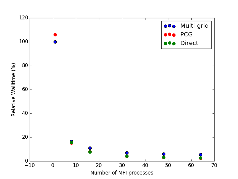
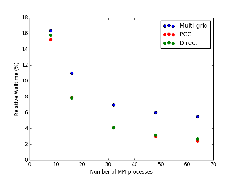
To summarize, one should use the Multi-grid solver if running in serial and either the Parallel Conjugate Gradient or the Direct method if running in parallel. However, the memory footprint of the PCG method is much smaller than for the Direct solver, so in most cases PCG will be preferable of the two.
Analysis of the results
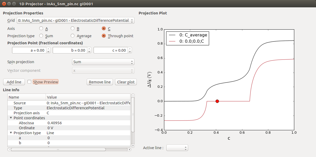
You can now plot the electrostatic potential. From the LabFloor, select the ElectrostaticDifferencePotential object contained in the file InAs_5nm_pin.nc. Afterwards, use the 1D Projector on the right-hand side and plot the average potential along the C axis.
In the calculation, you have used a gate potential of zero volt. Since you use Neumann boundary conditions you have an arbitrary vacuum level. To see the vacuum level of the left or the right electrode, plot the electrostatic potential at the edge. As projection type select through point and use the 0, 0, 0 fractional coordinates. This will now be added as a red line, in addition to the black line showing the average.
You can inspect the potential at the edge of the cell (edge of the vacuum region), in addition to the average plotted previously. From the plot you can extract the two vacuum levels, left = -0.28 V, right = 0.58 V.
The zero energy reference for this vacuum level is defined by the construction of the basis set. In the next section, you will learn how to align the vacuum level with the Fermi level and the band edges of your device. By doing so you will be able to calculate the work function of your metal gate and finally tune it to match the work function of a gold gate, for example.
Finally, it is worthwhile to plot the electrostatic potential directly on top or your device configuration. Select the ElectrostaticDifferencePotential object and click on the Viewer (or drag and drop it on top of the Viewer icon:  ). Here, you can choose to plot it as an isosurface or as a cut plane. The figure below shows a 3D view of a cut plane along the CA plane where you can nicely see the atomic resolution of the electrostatic potential of your 60 nm InAs device.
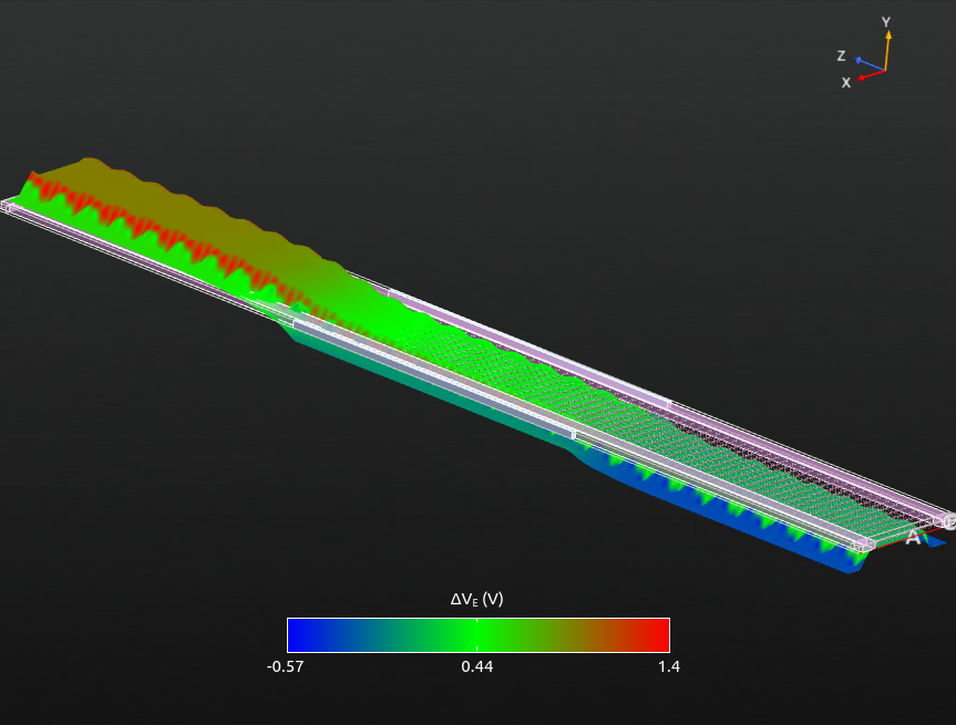
Fig. 47 3D view of the ElectrostaticDifferencePotential across the device.
Tip
If you wish to re-create the figure, you need to do the following:
Drop the ElectrostaticDifferencePotential object on the Viewer and choose Cut plane.
Click on Properties on the right.
Under Surface Properties change the value of 3D to 0.03.
In the bottom left, click the button AC.
On the lab floor, locate the DeviceConfiguration object, and drag it onto the cut plane window.
Use the mouse to re-orient the figure to your liking.
Defining the work function of the metal gate
Note
In the following, ‘gate’ usually refers to the entire gate region, and the gate voltage is thus applied to both metallic regions.
In order to calculate the metal gate work function you will need to align the vacuum levels extracted in the previous chapter with the Fermi level and the band edges of your InAs device. As described in the first section, you need to perform this operation since these levels are not related to each other within the definition of this Slater-Koster basis set.
At zero applied voltage between the left and right electrodes, the Fermi levels will coincide and the band diagram of the whole system corresponds to the one shown in the following figure.
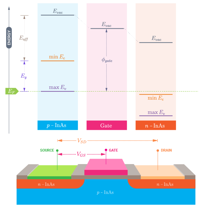
The choice of your zero energy reference is quite arbitrary. In the following, you will consider the Fermi level at zero bias to coincide with the zero energy in the scheme above, \(E_{F} = 0\) eV. In order to set the vacuum levels, and in particular the left electrode vacuum level, you need to know:
The positions of the band edges, valence band maximum (VBM) and conduction band minimum (CBM), see the next section: Band gap and band edges.
The electron affinity (\(E_{aff}\)) defined as the energy difference between the CBM and the vacuum level. This can be computed in a manner similar to the metal work function, as described in this tutorial: Green’s function surface calculations.
As a first approximation you could use the values reported in the literature for InAs which are: 4.55 eV [2] and 0.451 eV at 0 K [1] for the electron affinity and band gap of InAs, respectively. However, the band gap and the electron affinity of your device can be quite different from the bulk value due to finite size effects. Here, you will instead use a calculated value of the electron affinity for a 2d-InAs slab of 5.09 eV, and you will determine the band edges and band gap of your gated device.
Band gap and band edges
You can easily plot the density of states across your device from the DeviceDensityOfStates, LocalDeviceDensityOfStates or ProjectedLocalDeviceDensityOfStates analysis objects available in QuantumATK. Here you will use the ProjectedLocalDeviceDensityOfStates tool available from the QuantumATK 2015 release, and which we already calculated previously. Select this object on the LabFloor and click on the Projected Local Density of States plugin on the right-hand side to open the corresponding window. In order to highlight the band gap and band edges, the figure above has been created by narrowing the data range for the DDOS values to 0-0.02 1/eV Å3 (click on the Data range button in the upper right corner).
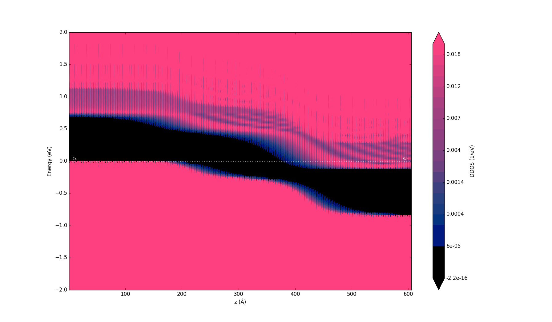
This plot nicely shows the electronic structure across the full length (about 60 nm) of your device. In particular, you can immediately see the band bending due to different doping types in the left and right parts of the device.
From this plot, you can extract the band gap of 0.68 eV by zooming in on the p-doped region, where the position of the VBM is exactly on the Fermi level.
Tip
The projected local density of states window also shows the corresponding transmission spectrum, if present in the LabFloor, on the left-side of the PLDOS plot.
Tuning the work function of the metal gate
You now have all the ingredients to define the electronic structure of your device and align the Fermi levels, vacuum levels and band edges.
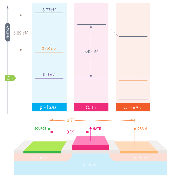
From your actual set-up you thus have a metal gate with an intrinsic work function of 5.5 eV. This can be calculated as: \(E_G + E_{aff} - E_{vac,left}\). Note that the value for the vacuum level from earlier needs to be multiplied by -e before being inserted here. This value may correspond to the work function of Pt, 5.12/5.93 eV as reported in the CRC Handbook [3].
You can now tune the work function of your metal gate by applying a gate voltage to adjust to your experimental conditions. In particular, you can lower or increase the metal gate work function by applying a positive or negative gate bias, respectively.
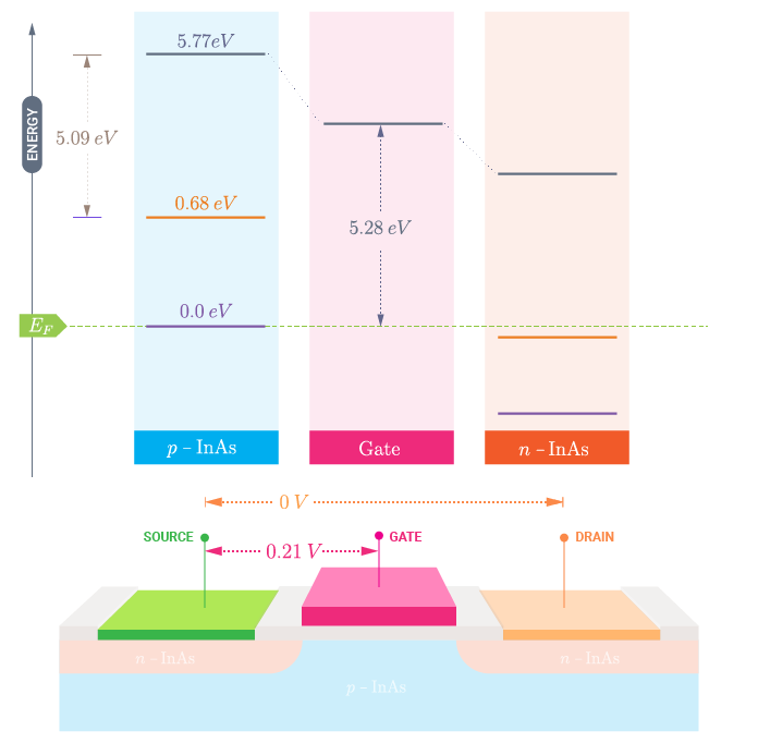
For example, in case of a gold gate, with a work function of 5.28 eV [3], you will need to apply a +0.21 V gate voltage to have the correct energy reference for a grounded gold left electrode.
In the next chapter you will perform the gate scan at finite bias.
Performing a gate scan
You will now apply a source-drain voltage, V(SD), of -0.5 V and perform a gate scan. To this end use this script: gatescan.py, which uses the converged zero bias calculation as a starting point to generate converged calculations at each bias. Again, you can get a good speed up by parallelizing over several MPI processes.
You can now analyze the behavior of the electrostatic difference potential as a function of the gate bias. From the figure below you can see that the effect of applying a positive gate voltage is to shift up the potential at the metal gates.
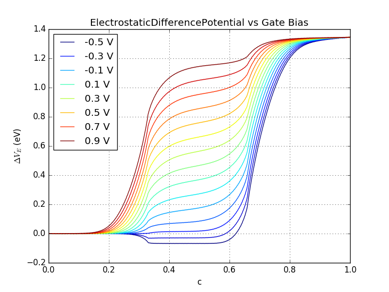
Fig. 48 ElectrostaticDifferencePotential vs gate bias between -0.5 and 0.9 V. You can recreate the plot with this script: plot-gatescan-edps.py.
You can now calculate the transmission spectra for the converged configurations. This script will calculate the transmission spectrum at each gate voltage: transmission.py. This calculation can be performed with high parallelization. We will return to these results after a small detour to look at a system where there is a smaller doped region on the right side, towards the Drain.
Simulating a drain underlap
You will now simulate a system where there is a drain underlap, i.e. the atoms 10 nm to the right of the central gate are not doped. In the following figure, this situation is shown, by comparing sketches of the doped areas in both the normal p-i-n case and with a drain underlap.
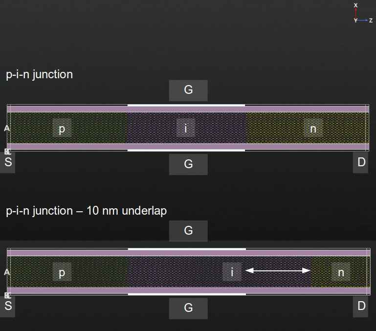
Fig. 49 Structure of the gated InAs p-i-n device and of the same device with a drain underlap of 1 nm. Source (S), drain (D) and gates (G) are indicated.
In the calculation, the drain underlap is created by only adding a compensation charge for the last 860 atoms. You can set up this system in several ways:
If you are using the script you can set
n_central_right = 860.Using the direct procedure of selection in the Builder is a little harder in this case, because we do not have the gate to use as guideline for the edge of the region. On the other hand, it is not that important to hit exactly in the middle in this case.
You can also manually modify the tags for the n-doping in the script and delete the first half of the indexes (should be 3484 to 4344).
Also change the output filename to InAs_5nm_pin_du.nc. Once the calculation is finished, you can repeat the gatescan with the calculation of the electrostatic difference potential and transmission spectra as explained in the previous section.
Analysis of the results
We can now plot the I-V curve for both the regular p-i-n junction, and the system with a drain underlap, using an applied gate voltage from -0.5 V to 0.9 V. In the figure, the gate voltage is shifted to account for the work function of the metal gate, as explained previously. We also calculate the subthreshold slope, as indicated by the dashed black lines. We get values of 58 mV/dec for the regular device and 43 mV/dec for the device with a drain underlap. You can generate the plot yourself with the following script: plot-iv-curve.py
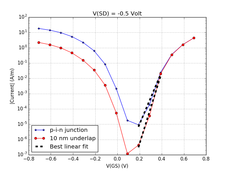
Fig. 50 Gate-Source bias, V(GS), dependence of the current for symmetric InAs-2D p-i-n junction. The gate voltage is reported relative to a gold metal gate with a work function equal to 5.28 eV, i.e. V(GS) is shifted by 0.21 V (see the section Band gap and band edges.
Finally, you can perform the projected local density of states analysis to any of the configurations saved in gatescan_conf.nc or gatescan_conf_du.nc as explained in the previous section. In the figure below the PLDOS of the p-i-n junction and the one with the 10nm drain-underlap region are shown.
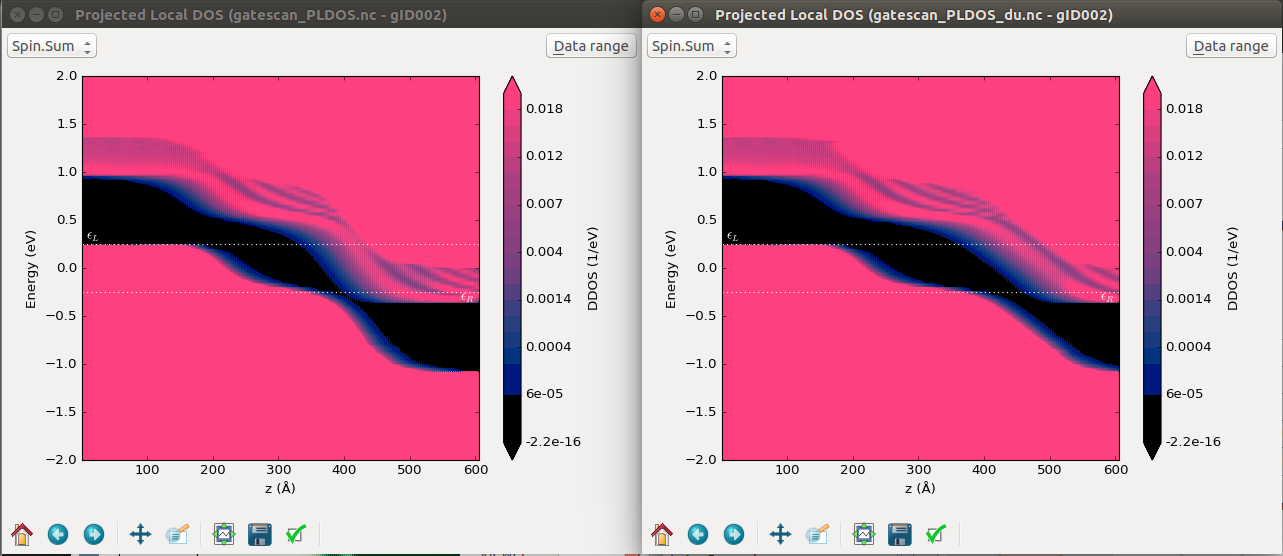
Fig. 51 Projected density of states across the 60 nm p-i-n junction device (left) and with 10 nm drain-underlap region (right). A -0.5 V source-drain bias voltage and a 0.4 V gate voltage are applied, respectively. The 0.4 V gate bias corresponds to the points around 0 V(GS) in the previous figure.