NiSi2–Si interface
In this tutorial you will study a doped NiSi2-Si interface and its electronic transport properties. In particular you will:
create the device to calculate the transport properties of such interface;
learn how to add the proper doping to simulate a real device;
analyze the results in terms of electrostatic potentials, electron density and density of states, by using the tools included in QuantumATK.
Warning
If you are running this tutorial with QuantumATK v2017.2 or higher, be aware that
you will have to set explicitly the electronic temperature to \(T = 300\ \mathrm{K}\)
in all the electronic structure calculations performed for either a BulkConfiguration
or for a DeviceConfiguration, in order to reproduce the results presented in the case study.

Create the NiSi2/Si device
Create a new empty project and open the Builder (icon
 ).
).The first thing you have to do is to create a device configuration starting from the LDA-optimized NiSi2-Si bulk configuration of the interface. The latter can be downloaded here:
Interface.py.Note
You can learn how to create an interface from the tutorials Building a Si-Si3N4 Interface, Graphene–Nickel interface and Building an interface between Ag(100) and Au(111).
Use to add the newly downloaded interface structure to the Stash.
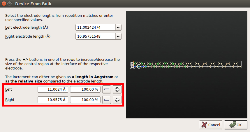
Go to to create the device configuration from the bulk configuration.
Do not modify the electrode lengths but increase the size of the central region on the left and right side by 100% compared to the size of left and right electrodes, respectively.
The screening region
What should be your doping concentration? In principle, you can use the experimental one. However, you need to be very careful about another quantity: the width of the depletion layer, usually denoted as \(W_D\), which is related to the screening length of the semiconductor.
The width of the depletion layer depends on:
the dielectric constant of the semiconductor;
the doping concentration (number of carriers);
the potential barrier at the interface;
the applied voltage.
The plot below shows typical values of \(W_D\) for a metal-semiconductor junction (as reported in [1] pag. 119) as a function of the doping concentration \(N\).
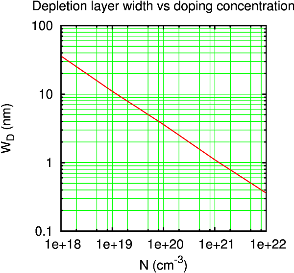
For the purpose of your simulations you need to ensure that the silicon part in the central region is larger than the width of depletion layer. Throughout this tutorial you will use doping concentrations ranging from 1019 cm-3 to 1020 cm-3. This means that you will need a silicon region of about 30 Å to 100 Å wide. A good way to check if your system is large enough is to plot the Electrostatic Difference Potential along the device (see below).
Note
The screening length of a metal is much smaller that that of a semiconductor, only few atomic layers. Therefore, you can keep the NiSi2 side much shorter than the Si side to save computational time.
Note
In this tutorial you will use a highly doped device. The electronic transport properties of this device are significantly different from those a device with a much lower doping concentration, e.g. 1017 cm-3 or 1018 cm-3. As you just learned, if you want to simulate a device with a lower doping concentration, you will also need a much longer device.
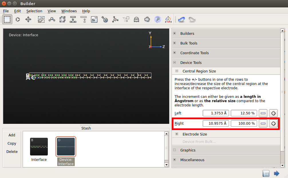
Increase the length of the central region
Select again the device structure from the Stash.
Click on and increase the dimension of right side (silicon) by 100% compared to the electrode length.
Send the structure to the Script Generator using the
 button to calculate some interesting properties of
the undoped device.
button to calculate some interesting properties of
the undoped device.
Set-up the calculation for the undoped device
Once you have sent the structure to the Script Generator, you are ready to set-up the calculation. Add the following blocks to the script by double-clicking them:
 New Calculator. Double-click on it to modify the following parameters:
change the exchange correlation parameter to MGGA.
k-point sampling: 5x5x100 k-point sampling.
“SingleZetaPolarized” basis set for both Si and Ni atoms.
You need to set manually the TB09-MGGA c parameter in the Editor. Locate the exchange-correlation block in your python script and modify it as follows:
exchange_correlation = MGGA.TB09LDA(c=1.09368541059162)
Attention
We have obtained the c parameter self-consistently from a single-point calculation performed using the TB09-MGGA functional on the LDA-optimized structure of bulk silicon. If needed, you can obtain more details about how to obtain the c parameter or how to fit it from the tutorial Meta-GGA and 2D confined InAs. We have also compared the band structure of silicon at LDA and TB09-MGGA level of theory:
Figure 1: Band structure of bulk silicon computed using LDA (left) and TB09-MGGA (right).
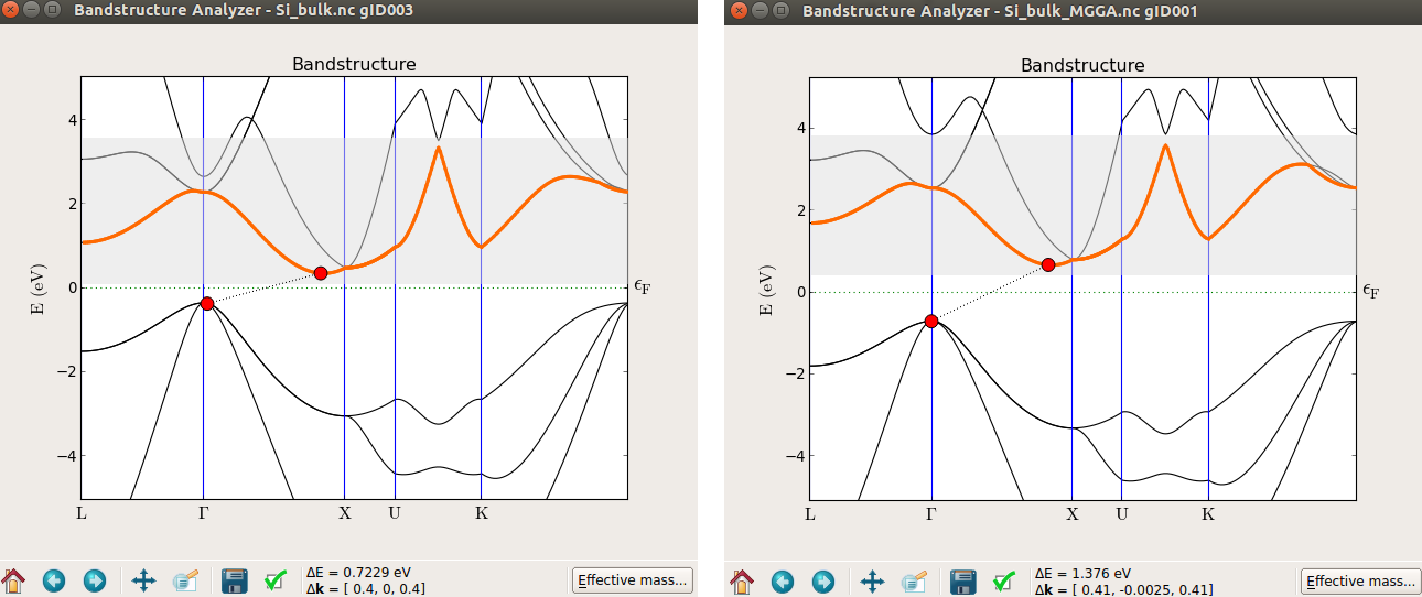
From the picture it can be seen that the band structures are similar but the band-gap obtained using TB09-MGGA is closer to the experimental value (1.17 eV).
 Analysis. In the menu that appears, choose the following analysis
objects and modify the default parameters as shown below:
Analysis. In the menu that appears, choose the following analysis
objects and modify the default parameters as shown below:ElectrostaticDifferencePotentials
ElectronDensity
ElectronDifferenceDensity.
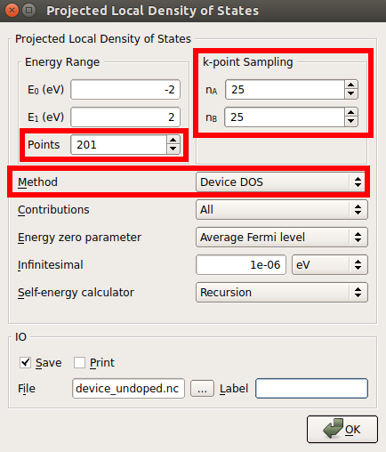
- ProjectedLocalDensityOfStates.
25x25 k-points sampling
201 energy points
Choose the Device DOS method.
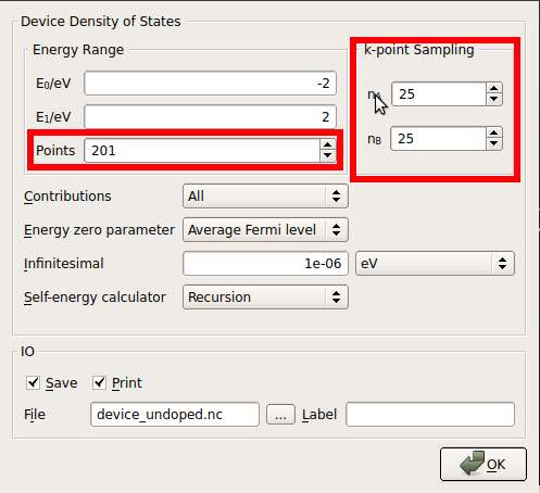
- DeviceDensityOfStates.
25x25 k-points sampling
201 energy points.
Change the name of the default output file to
device_undoped.hdf5and save the script with the same name,device_undoped.py. The Script Generator panel should look as in the figure below.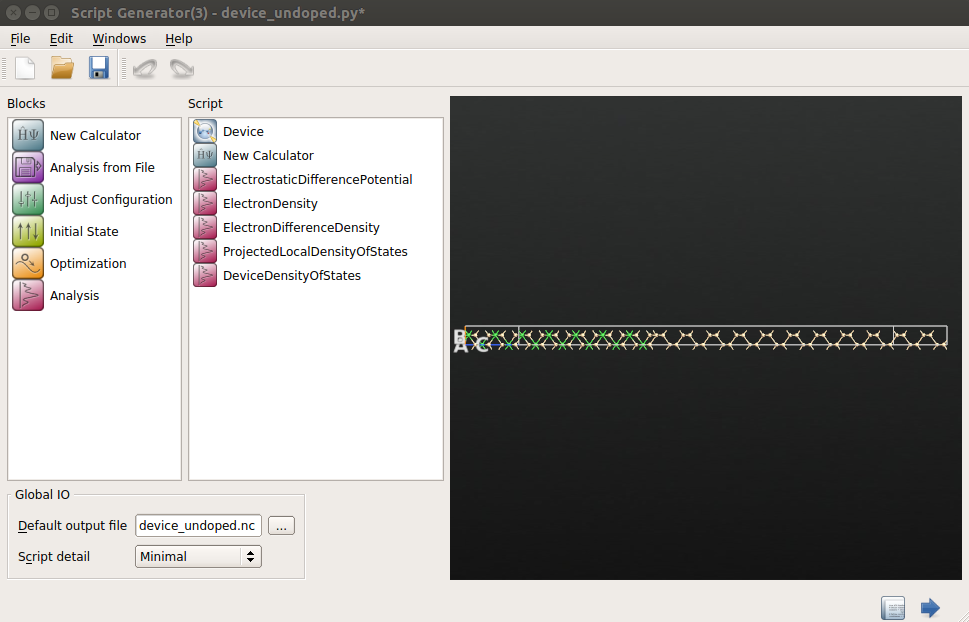
Send the script to the Job Manager and run it. The entire job will take around two hours by using 4 MPI processes. The calculation of each DOS takes around four hours on a single processor.
Note
The DOS calculations take quite a lot of time, especially with a 25x25 k-points sampling. You can reach reasonable good results also with a smaller mesh, e.g. 15x15 k-points. You can also run the DOS analysis at a later stage by reading the converged device configuration.
Dope the device
In the Stash, copy and paste the device configuration and rename it as
n_doped_1e19.Select the semiconductor atoms using the mouse by drawing a rectangle.
Go to .
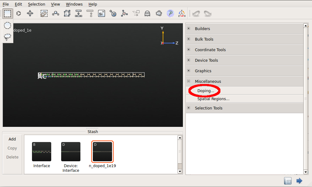
In the Doping panel that shows up set the doping as shown in the figure below.
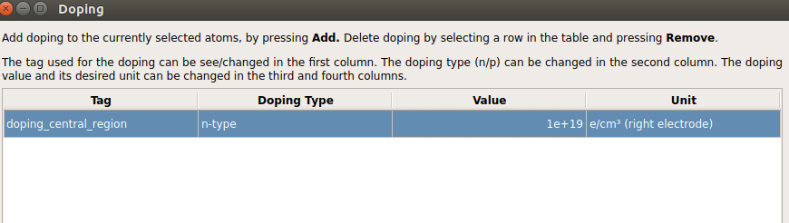
Close the Doping panel and send the structure to the Script Generator.
Set up the calculation as for the undoped device and run the script.
Repeat the same steps for the p-type doped (1019 cm-3 and 1020 cm-3) devices.
Analysis of the results
Once the calculations are finished, we are ready to analyze and compare the results obtained from the four calculations above.
Electrostatic difference potential
The electrostatic difference potential (EDP) corresponds to the difference between the electrostatic
potential of the self-consistent valence electronic density and that obtained from a
superposition of atomic valence electronic densities (see also the Reference Manual, ElectrostaticDifferencePotential). The analysis of the averaged EDP along the C axis of the device allows to see if the device is long enough, i.e. if the potential drop due to the interface is fully screened in the electrode regions.
In the LabFloor, select the four Electrostatic Difference Potentials objects obtained for the undoped and the three doped devices by holding Ctrl, and click on the 1D Projector tool.
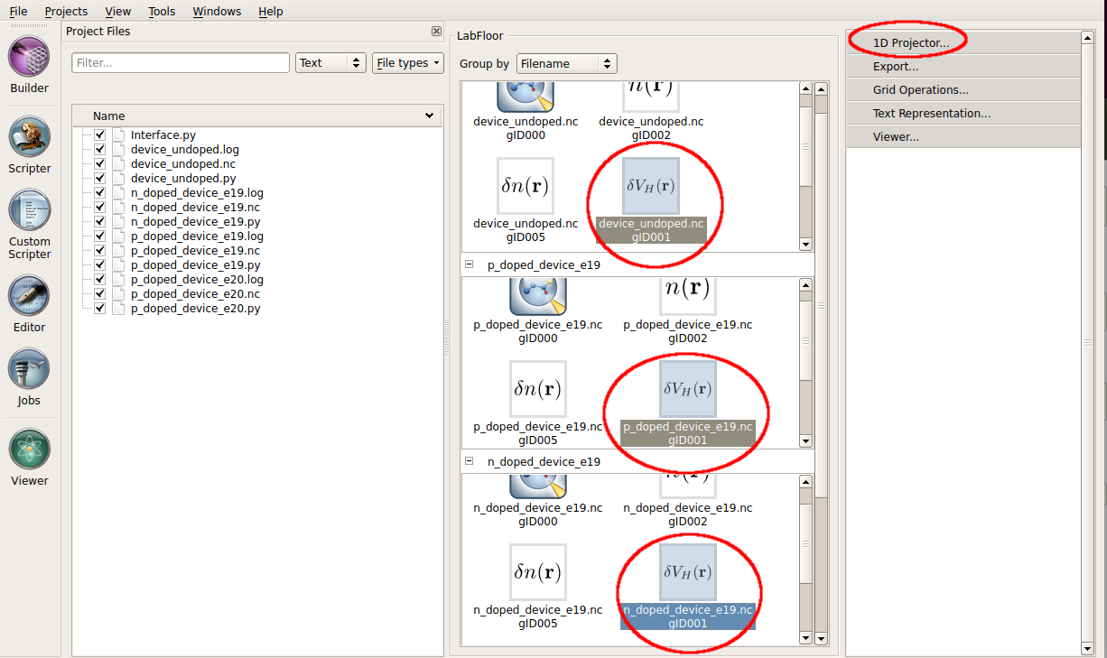
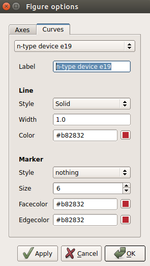
In the window that shows up, plot the average of the three potentials along the C direction as shown in the figure below. Right click in the graph and choose Figure options to change the legend.
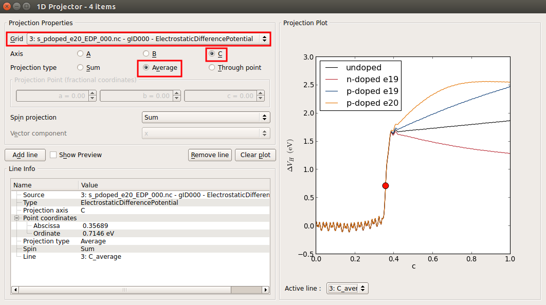
This plot shows that the device is not long enough for the undoped device and for those at a doping of 1019 cm-3. (see below the convereged EDP calculated for the longer device at an n-type doping of 1019 cm-3). The EDP of the p-type doped device at a doping of 1020 cm-3 is the only one showing the correct behaviour: it can be seen that the EDP it is flat in the electrode extension region (close to c = 1). The interface is located around the fractional coordinate c = 0.35, although it is better to say that the silicon atoms in contact with the Ni atoms are located at this coordinate since the interface is not simply a infinite thin 2D plane but correspond to a thick region of your device.
Electron Difference Density
Electron Difference Density (EDD) is the difference between the self-consistent valence electronic density and the superposition of the atomic valence electronic densities.
Use the script provided (download the script here:
edp_macro_avg.py) to plot the macroscopic average of the EDD.Write the following commands in the terminal:
atkpython edp_macro_avg.py file.hdf5
where
file.hdf5is the name of one of the HDF5 output files obtained from the device calculations.
Figure 2: Macroscopic average of the EDD of the undoped device (left) and of the n-type doped device (right).
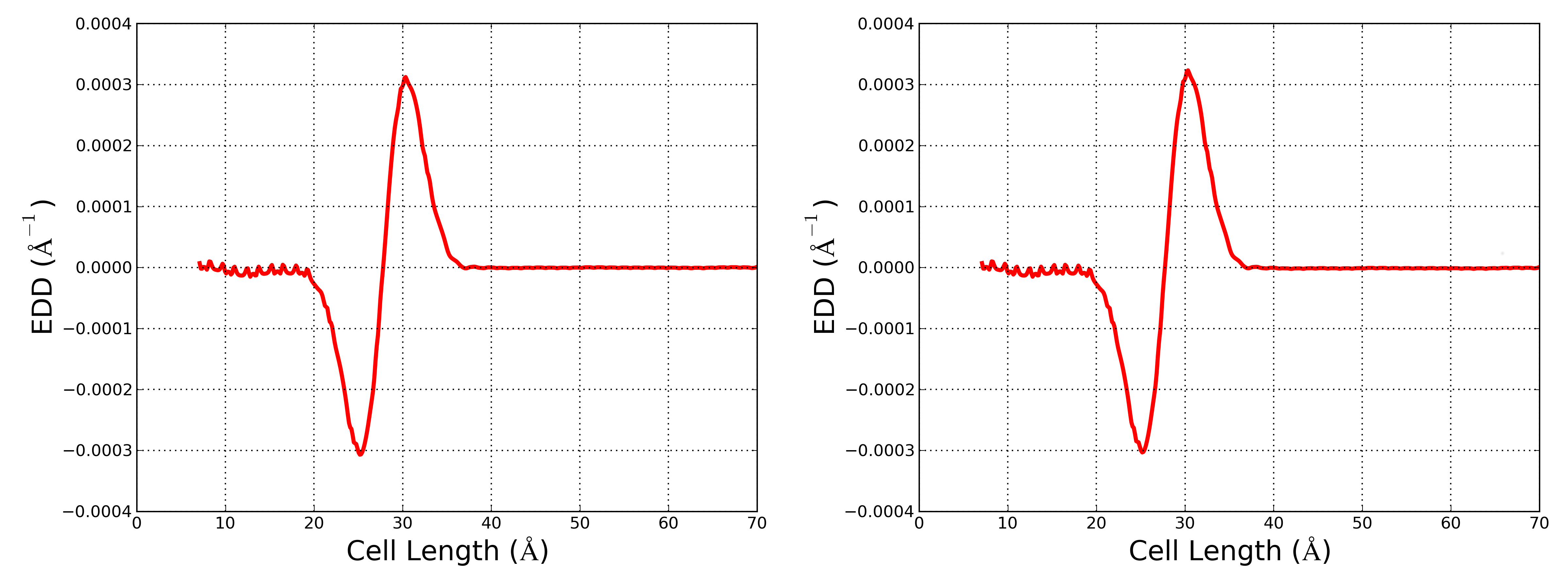
These two plots show the presence of an interfacial dipole which changes (although the change is small) unpon changing the doping in the semiconductor.
Electron density difference (doped - undoped)
You can analyze the difference in electron density between two device configurations in the following ways:
3D Analysis
Select the ElectronDensity objects of the following configurations from the LabFloor:
undoped device.
n-doped device (1019 cm-3)
Click the Grid Operation plug-in on the left-hand side of the LabFloor.
In the formula editor, insert “B1-A1” and click View to visualize the isosurface of the electron density difference.
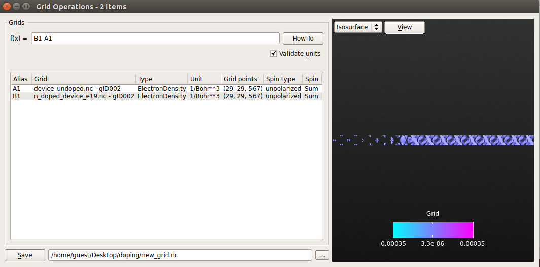
Save the generated density difference in a
new_grid.hdf5file.
1D Analysis
Use the provided script to plot the macroscopic average of difference between the n-type doped and the undoped configurations.
Open the script and modify the line:
ax.set_ylabel(r'EDD ($\AA^{-1}$)', fontsize=20)
as follows:
ax.set_ylabel(r'B1-A1 ($\AA^{-1}$)', fontsize=20)
Run the script as shown previously:
atkpython edp_macro_avg.py new_grid.hdf5
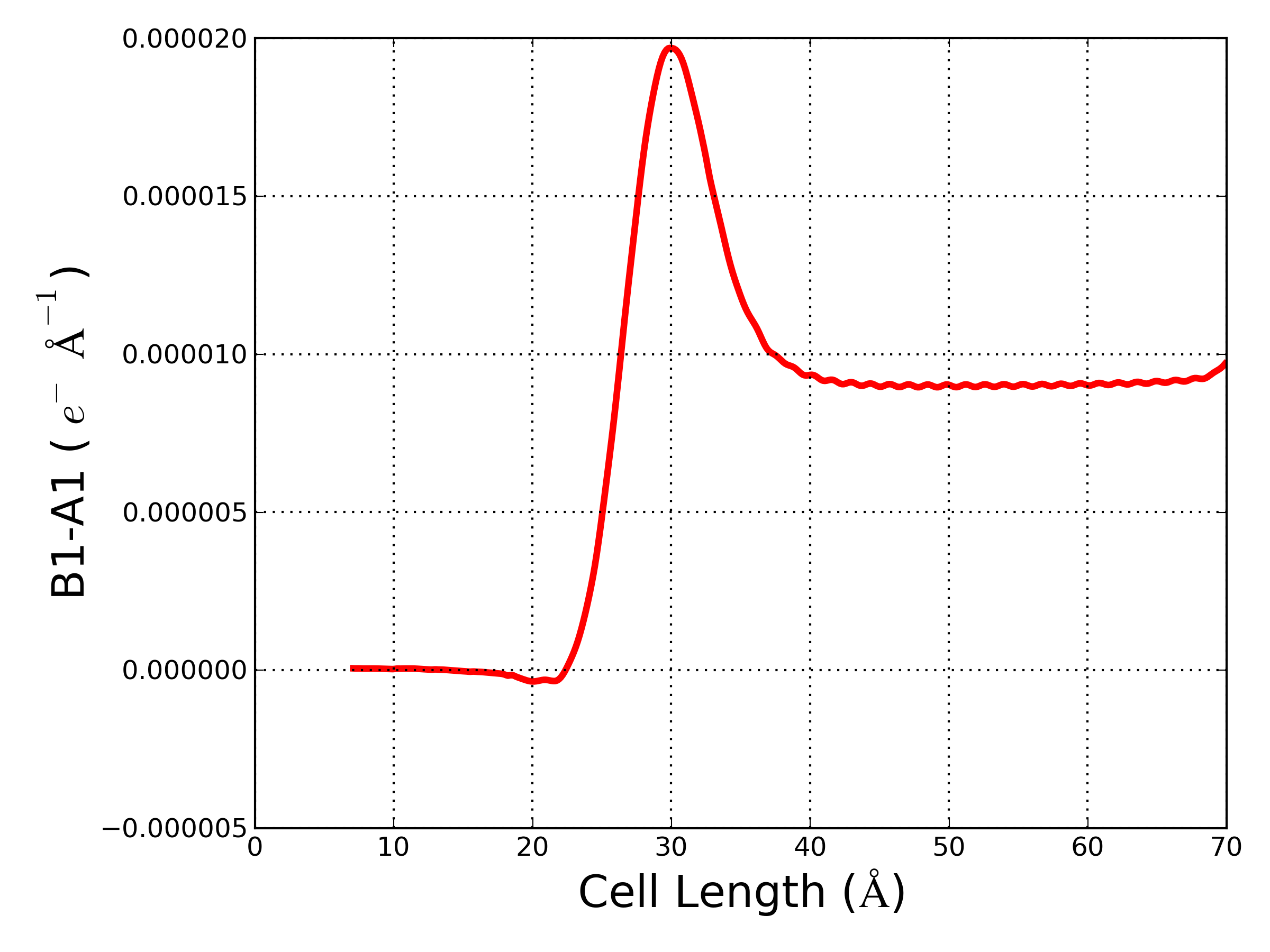
The plot shows the difference B1-A1 between the electronic densities of the n-type doped (B1) and undoped (A1) devices. B1-A1 > 0 e- Å - in the semiconductor region due to the extra electrons added to the silicon in the n-type doped device. Furthermore, the value of B1-A1 increases when approaching the interface, which can be understood taking into account the change of the interfacial dipole due to doping.
Density of states (DOS) analysis
In this tutorial we have computed two DOS analyses.
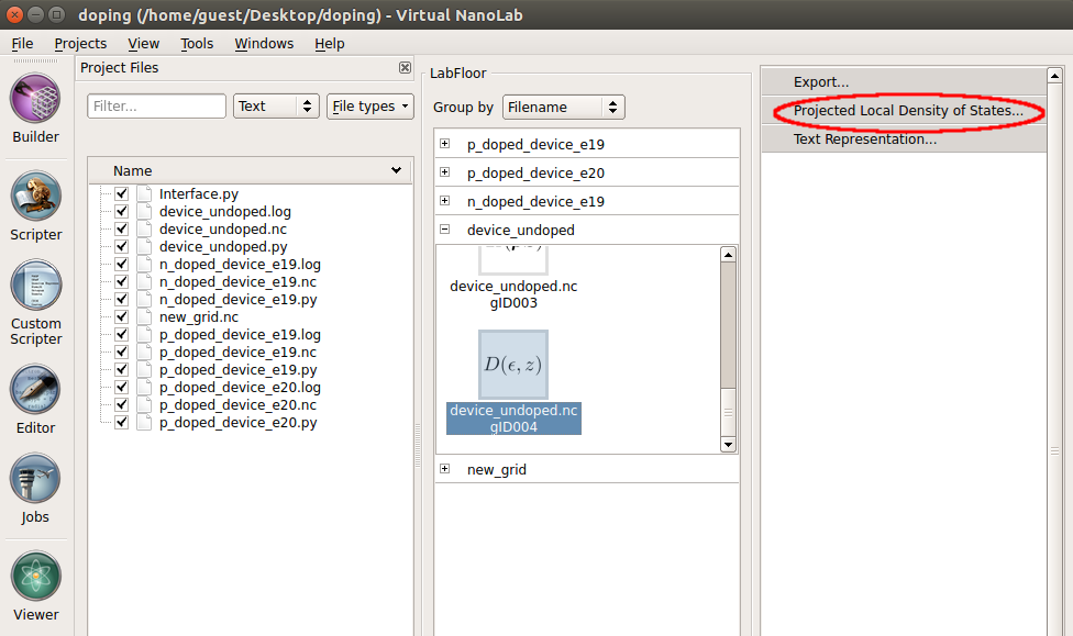
Projected Local Density Of States
Select the Projected Local Density Of States object of the undoped device from the LabFloor.
Click the Projected Local Density of States plug-in:
You will obtain the following plot:
The abscissa indicates the Cartesian coordinate of the central region along the C direction. In this case, the interface is located around 27 Å. The energy on the Y-axis is relative to the Fermi energy. The color bar indicates the DOS amplitude.
It is clear from this plot that:
The left side of the device is metallic, NiSi2;
The right side is a semiconductor with a band gap that resemble that of bulk undoped Si;
There is a wide region of silicon atoms which show gap states induced by the metal-semiconductor interface. These are called metal-induced gap states (MIGS).
Follow the same procedure to plot the projected local DOS of the n-doped device.
Note that in this case the Fermi level lies at the bottom of the silicon conduction band due to the doping of the semiconductor.
Device Density Of States
This tool allows the analysis of the density of states projected onto the atomic sites of the device.
Select the Device Density Of States object of the undoped device in the Labfloor.
Click the 2D Plot plug-in and the window that appears will show the 2D plot of the total density of states together with a 3D view of the device.
Navigate to the 3D view and select the atoms close to the interface by drawing a rectangle with the mouse as shown below.

The 2D plot now shows the projected density of states onto the selected atoms. It is possible to see the presence of MIGS around the Fermi level.
Select the silicon atoms close to the electrode as shown below:
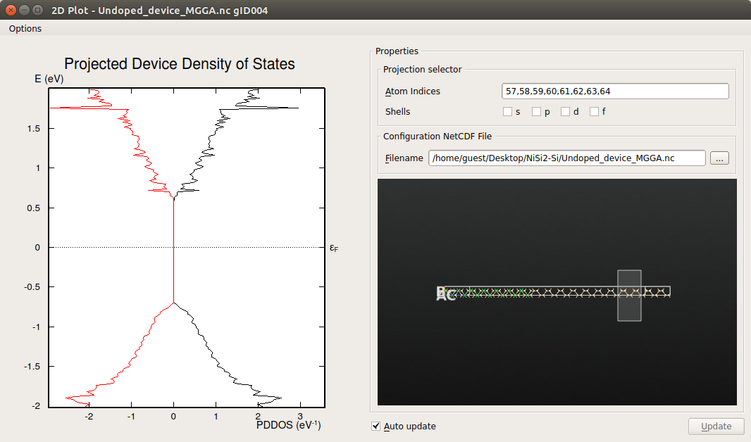
It can be seen that close to the silicon electrode the MIGS have disappeared and the electronic structure presents a band-gap similar to that calculated for bulk silicon, in agreement with the results obtained from the analysis of the projected local DOS.
Finite-bias calculations
In this section we will calculate the IV curve for a n-type doped device (1019 cm-3).
As we have already mentioned, the device used above is not long enough for this doping concentration.
In this section, we will perform the finite-bias calculations using a 100 Å long device.
We have increased the lenght of the device following the steps described in the Increase the length of the central region
section. You can download the structure here (long_ndoped_e19_ivcurve.py).
Set up the IV curve calculation
Send the structure to the Script Generator and add the following blocks to the script:
- New Calculator : Set the parameters as for 0 Vbias calculations.
- IV curve: Change the following default parameters as in the figure below:
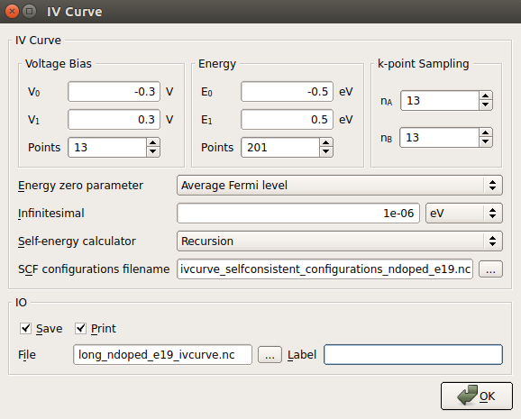
It is worth adding some comments regarding the meaning of the most important parameters:
Voltage Bias : 13 different calculations will be performed at Vbias = 0.0, -0.05, -0.1, -0.15, -0.2, -0.25, -0.3, 0.05, 0.1, 0.15, 0.2, 0.25 and 0.3 V, in this exact order. Vbias is defined as VL - VR.
Note
Each calculation will use the self-consistent configuration of the previous one as starting guess. This procedures improves quite a lot the convergence.
Energy : These parameters refer to the enery range and the number of points within this range at which the transmission spectra will be calculated at each bias voltage.
Warning
The convergence of the energy range is very important when calculating IV curves! Check the Transmission spectrum convergence and The IV curve object analysis sections.
k-point Sampling : This is the k-point mesh used to calculate the transmission spectra. It must correspond to a sampling for which the transmission curve is converged. In general a greater k-point sampling will be needed with respect to the one used for the SCF part.
Warning
The convergence of the k-point mesh can affect the calculated current! In this tutorial we have considered that at 13x13 the transmission is converged, check the Transmission spectrum convergence section.
IO File name : Change the default name if you are going to do more than one IV curve. This is the file in which all the converged configurations will be stored. As you will learn in the Post analysis of finite-bias calculations section, you can use this converged states to:
re-calculate all, or selected transmission spectra with different parameters (k-point sampling, energy range,…)
perform additional analysis at any specific bias (DOS, electron density, effective potential, …)
extend your bias range by restarting from a well converged finite bias calculation.
Once you have set all the parameters, you are ready to send the script to the Job Manager and run the calculation. This calculation will take around ten hour using 4 MPI processors.
Transmission spectrum convergence
Two parameters are very importat to determine the convergence of the transmission spectrum:
Number of energy points: The first parameter you can tune to improve the balance between the precision of your transmission and computational efficiency is the number of energy points used to evaluate the transmission spectrum. Ideally, the range of the transmission spectrum should span at least the entire region where the spectral current is finite. In the present case the minimum range would be between +0.1 eV and +0.4 eV (see below). However, it is often safer to consider a larger and symmetric energy range.
K-points sampling: The second and most important parameter to consider is the k-point sampling used for the evaluation of the transmission spectra. As already mentioned, you usually need more k-points than for the DFT calculation, since the Green’s functions (which determine the transmission) have a stronger variation with k than the Fourier components of the electron density do. The plot below shows the IV curves at negative bias for the n-type doped device (at 1020 cm-3 doping concentration) calculated using different k-points samplings for the evaluation of the transmission spectra. In general, it is enough to converge the current at a specific applied bias within the range considered.
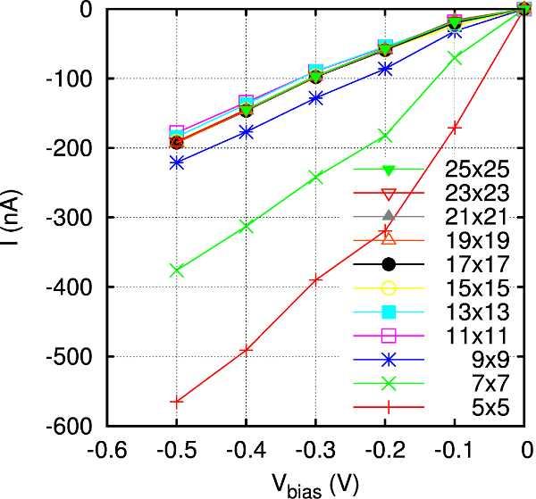
From this plot we can deduce that a 13x13 k-points mesh is good enough to give converged results, since the IV curve obtained at this mesh is very close to the one obtained at the highest sampling, 25x25.
Warning
This assessment have been done for n-type doped device with a concentration of 1020 cm-3. For a more rigorous study, an assessment for the device doped at 1019 cm-3 should be done.
IV curve object analysis
Once the IV curve calculation are finished we are ready to analyse the IVCurve object. You can find it loaded in the LabFloor.
Select the IVCurve object and click the IV-plot plug-in.
You will find the IV curve plot in the panel that shows up. Click on Additional Plots and you will get the dI/dV, transmission spectra and spectral current plots.
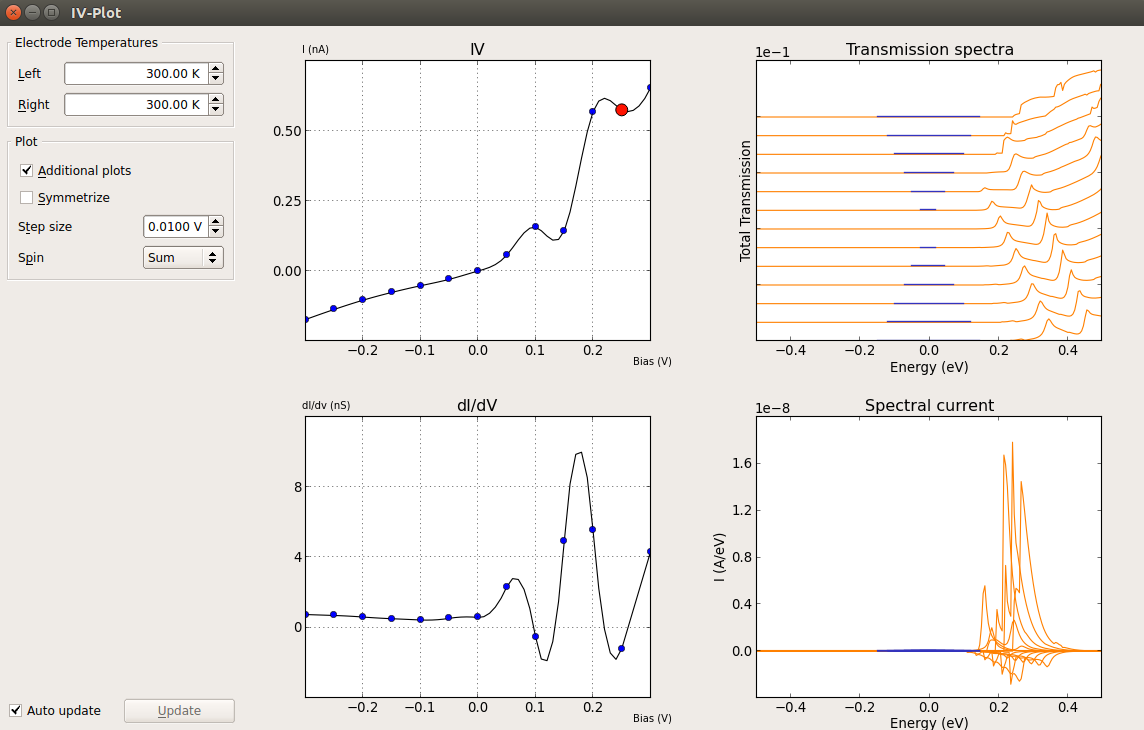
Important
The spectral current is the energy resolved current:
\(I(E) = e/h [T(E,\mu_R,\mu_L) (f (E -\mu_R) /(k_B T_R) - f (E - \mu_L)/(k_B T_L))]\)
This is the quantity which is integrated to get the current at a given bias. As such, it is good practice to check that the energy range set for the evaluation of the transmission spectra spans the entire region where the spectral current differs from zero. You can refer to the TransmissionSpectrum entry in the Reference Manual for more information on how the current is evaluated in QuantumATK.
Note
You can right-click on any of the plot windows to export the data and use your favourite utility to plot your results.
Post analysis of finite-bias calculations
As we have already mentioned, using the selfconsistent configurations (stored in
the ivcurve_selfconsistent_configurations.hdf5 file) it is possible to perform further analysis at any specific bias. In this section
we will explain how to inspect this objects and how to set-up the script for the additional analysis of a configuration.
Analysis of a single self-consistent configuration
Select a self-consistent configuration and click on the General info tab. In the panel that opens up, you can check the details of the self-consistent configurations. Once you have identified the configuration you are interested in, you are ready to set up the script.
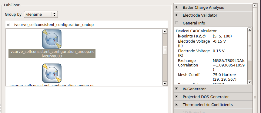
Go to Script Generator and add the Analysis from File block.
Double-click the Analysis from File block to open it and insert the name of the HDF5 file and the Object ID of the self-consistent configuration you want to analize.
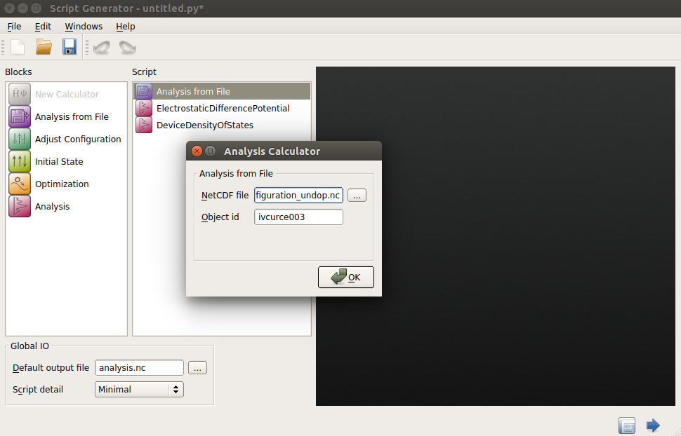
Add the analysis blocks you need to the script and once you have set the parameters of these additional blocks, send the script to the Job Manager to run it.
Analysis of multiple self-consistent configurations
Here we will show how to perform an additional evaluation of the EDP at different bias voltages starting from the self-consistent configurations obtained previously.
Identify the self-consistent configurations you want to analyze using the General info tab as explained in the previous section.
Use the provided script (
loop.py) to perform the analysis you want for multiple self-consistent configurations in the same calculation. Select the self-consistent configurations by including the relevant Object IDs in the id_list in the script.1id_list = [ 2 'ivcurve000', 3 'ivcurve001', 4 'ivcurve002', 5 'ivcurve003', 6 'ivcurve004', 7 'ivcurve005', 8 ] 9for id_item in id_list: 10 # Read the DeviceConfiguration 11 configuration = nlread('ivcurve_selfconsistent_configurations.nc', object_id="%s" %id_item)[0] 12 13 # ------------------------------------------------------------- 14 # Electrostatic Difference Potential 15 # ------------------------------------------------------------- 16 electrostatic_difference_potential = ElectrostaticDifferencePotential(configuration) 17 nlsave('analysis.nc', electrostatic_difference_potential)
Send the sript to the Job Manager and run the calculation.
Analysis of the IV curve
In this section we are going to analyze the EDP of several self-consistent configurations at different Vbias
and the projected local DOS of the self-consistent configurations at -0.3 V and 0.3 V. You can perform these analyses following the steps described above. You can download the required scripts here (l_ndoped_e19_EDP.py l_ndoped_e19_DDOS.py).
The IV curve obtained can be divided in two regions, “Forward Bias” (Vbias > 0 V) and “Reverse Bias” (Vbias < 0 V):
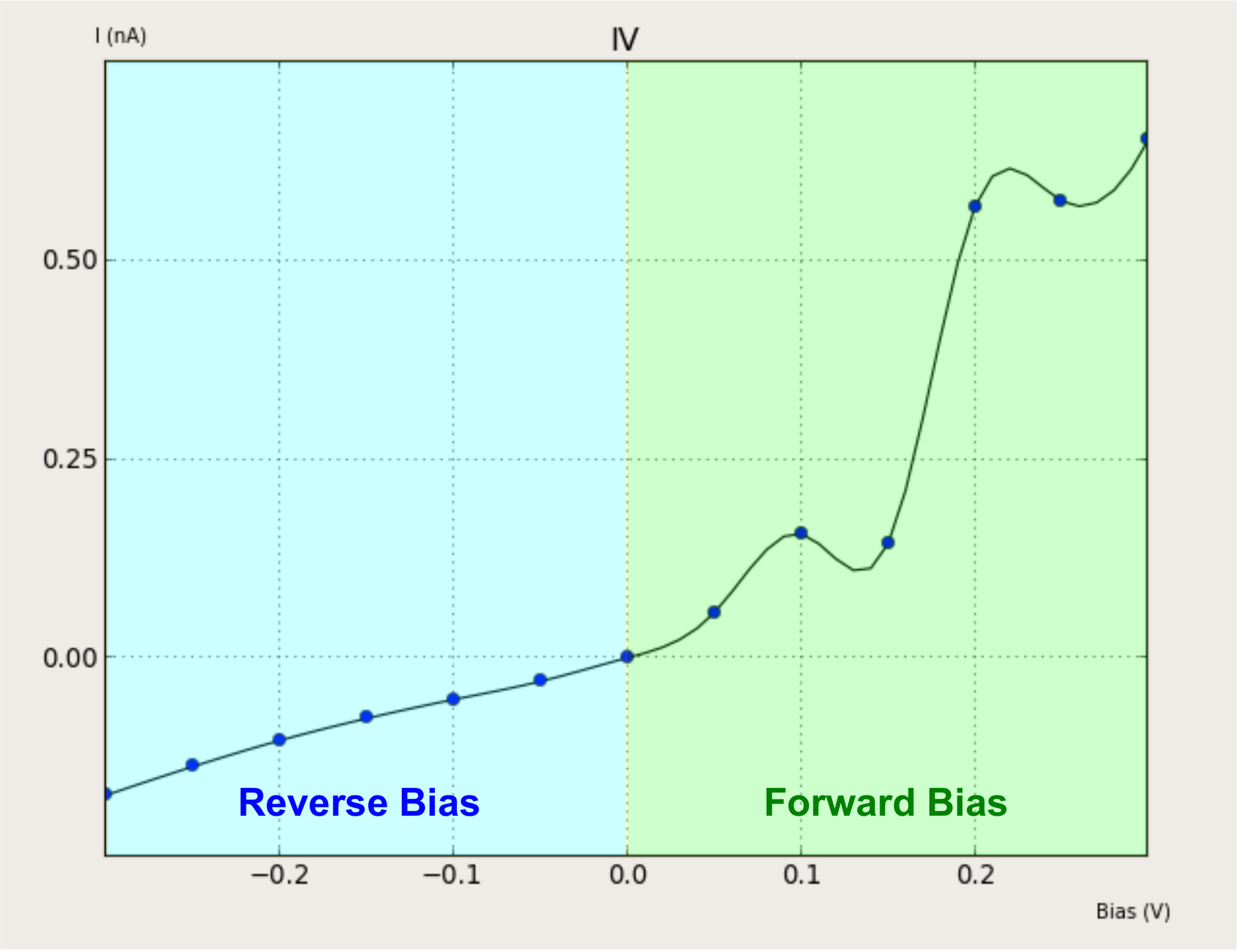
The IV curve shows that the reverse bias current is lower than the forward bias current. This can be undertood looking to the projected local DOS plots.
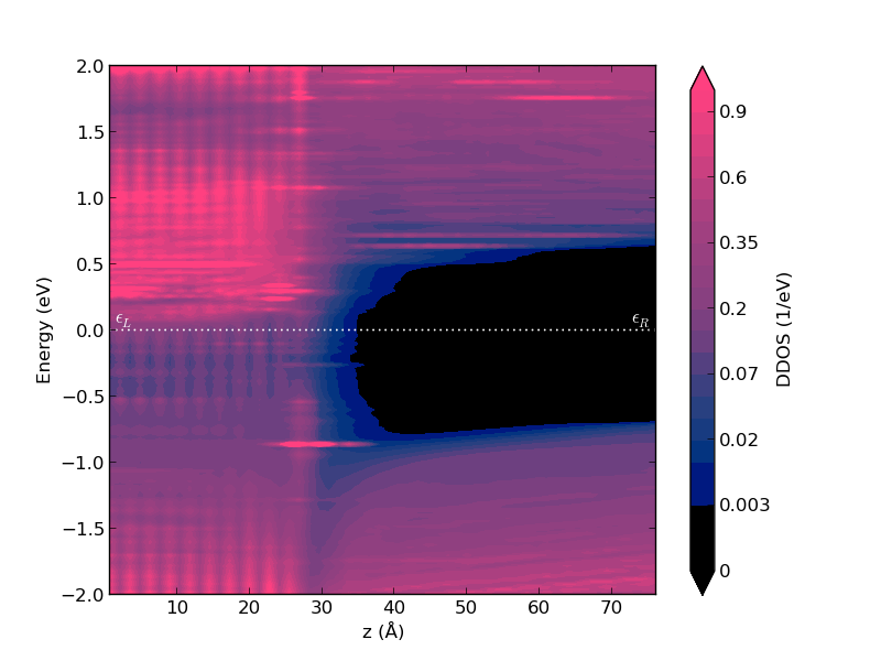
The figure below shows the projected local DOS at -0.3 V.
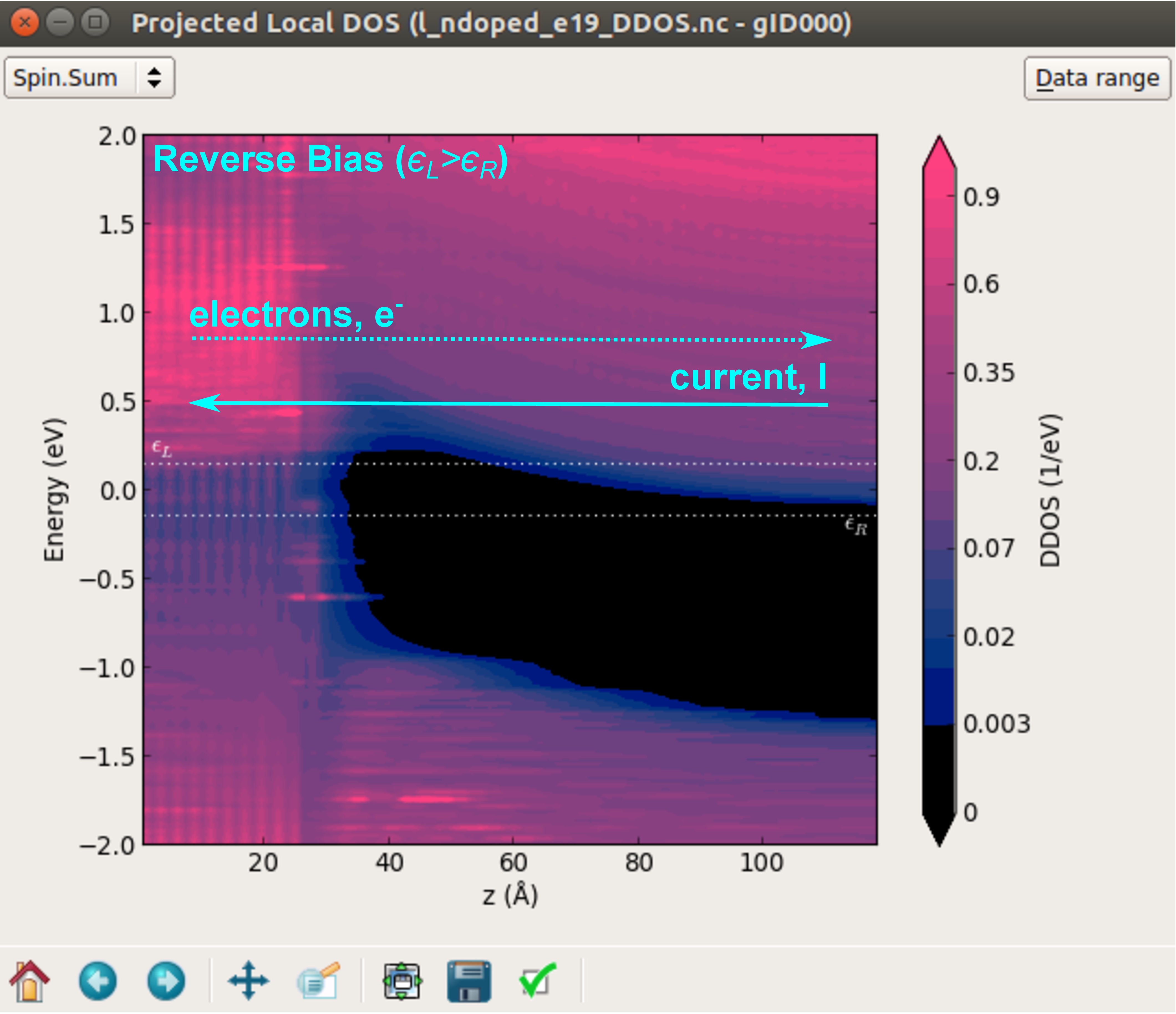
In reverse bias conditions, the chemical potential of the left electrode is higher in energy than that of right electrode. Consequently, there will be a net flow of electrons from the left to the right electrode, so that the current will propagate in the opposite direction. However, the electrons have to overcome a potential barrier at interface due to the presence of the depletion region, and consequently the current will be low.
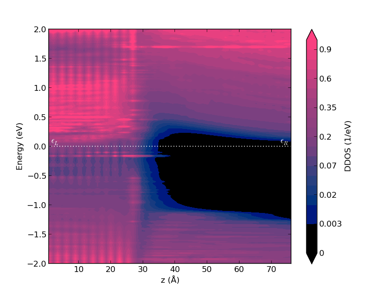
In the next plot we show the projected local DOS at 0.3 V.
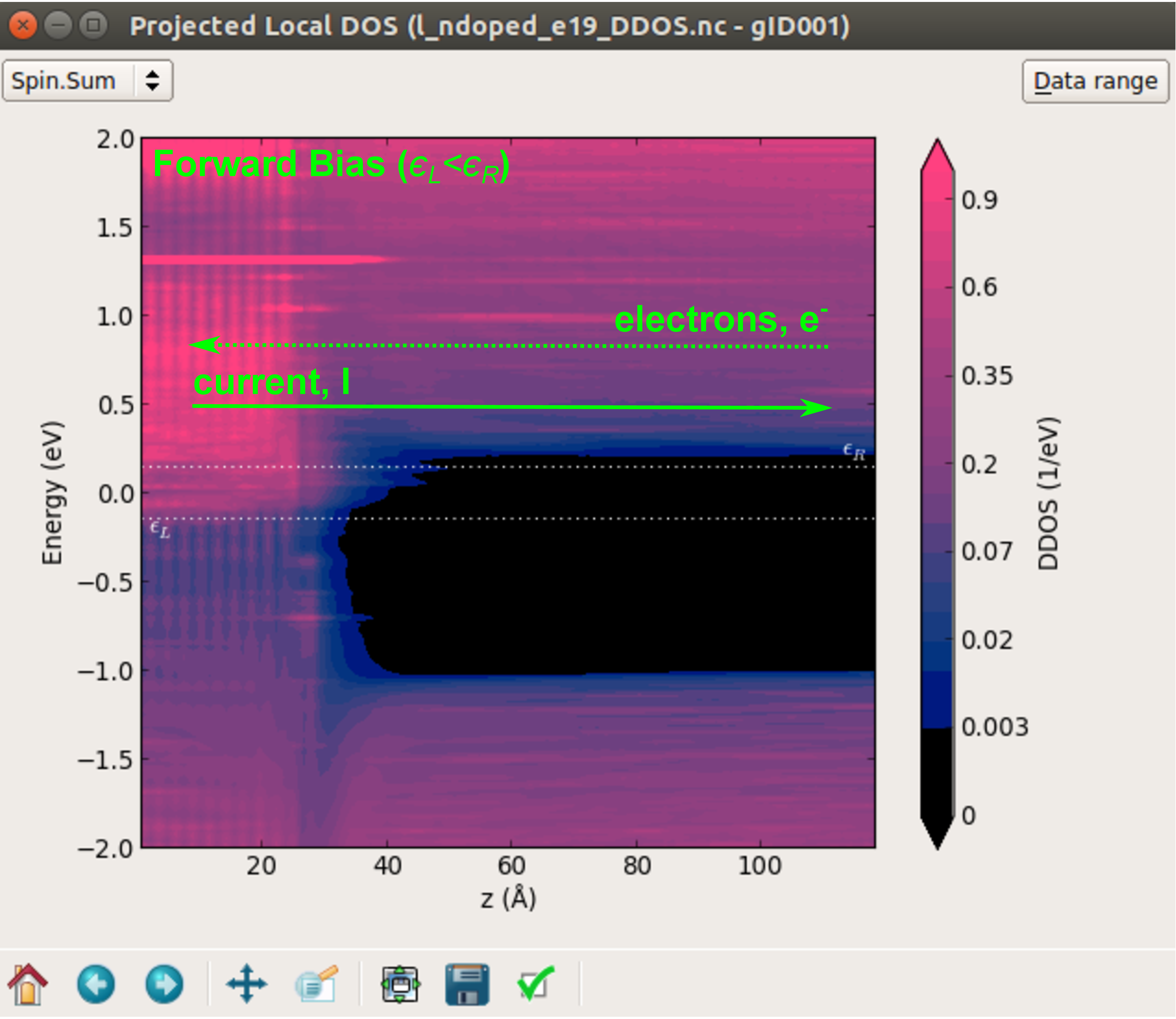
It can be seen that in forward bias conditions, the chemical potential in the right electrode is larger than that of the left electrode. Consequently, there will be a net flow of electrons from the right to the left electrode, so that the current will propagate in the opposite direction. However, at difference with the reverse bias case, here the electrons do not have to overcome any potential barrier, so that the current will be higher.
Finally, in the figure below the EDP along the the C axis of the long n-type doped device at different Vbias is shown:
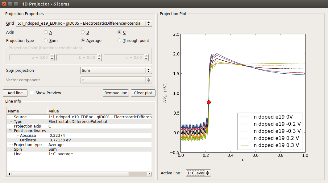
Notice how applying a bias has also an effect on the EDP and on the width of the depletion region.
Warning
In the above plot, the EDP profiles are relative to \((\mu_L + \mu_R)/2\), which is how the potential are defined in the calculation. For a more intuitive picture, one should plot the EDP profiles relative to \(\mu_L\).