Silicon p-n junction
In this tutorial you will:
Learn how to build a p-n junction device.
Learn how to study the current-voltage characteristic of such a device.
Compare two different methods: ATK-SE and ATK-DFT.
Analyze the electronic structure of the p-n junction by studying and plotting the device density of states at zero bias and at reverse and forward bias.
Silicon bulk: Slater-Koster vs DFT-MGGA
Open QuantumATK and create a new project by clicking on Create New. Give the project a Title (here: “Silicon”), select a folder for the project, click OK and then Open to start the project.

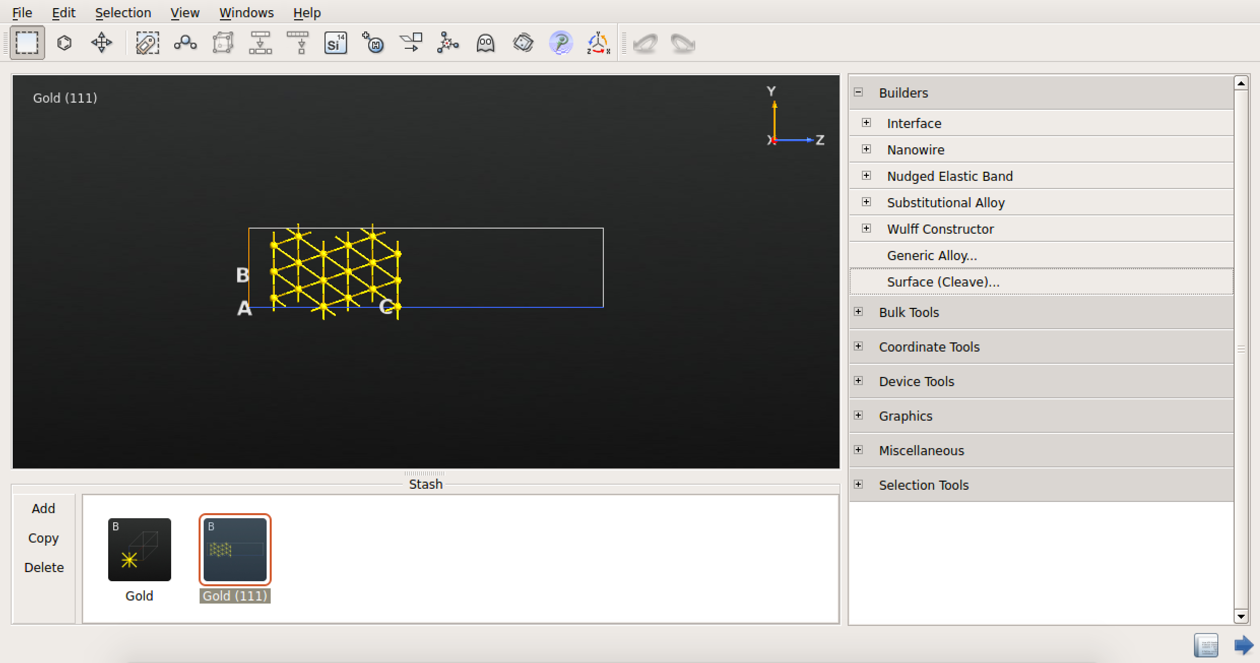
In the QuantumATK main window, click on the
 icon to open the Builder.
In the Builder, go to the Stash, click and from the menu navigate to and search for “silicon” in the search window. Then, select “Silicon (alpha)” and click the
 icon, or double-click its line in the list, to send it to the Stash.

Slater-Koster calculation
You will now set up an ATK semiempirical (ATK-SE) calculation using the Slater-Koster model Hamiltonian.
Send the bulk configuration from the
Builder to the  Script Generator using the
  button.
Add the following blocks to the Script by double-clicking the correspoding icons in the Blocks panel:
 New Calculator.
 .
.


Open the
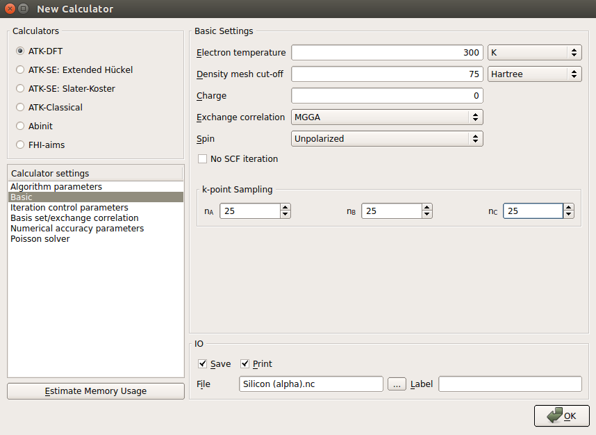
New Calculator by double-clicking it.Select the ATK-SE Slater-Koster calculator.
Use a 25x25x25 k-point sampling.
Uncheck the “No SCF iteration” box.
Select the “Bassani.Si” basis set.

In
Bandstructure, select the “L, G, X, U, K, G” Brillouin zone route and 401 points per segment.
Back in the
Script Generator, set the output filename to bulk_SK.hdf5, and send the script to the Job Manager using the button.
Save the script in the window that shows up and use the
 botton to run the job.
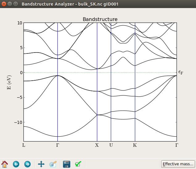
Once the calculation is done (it will only take a few seconds) you can find in the LabFloor your Bandstructure object, which is saved in
bulk_SK.hdf5:
Highlight the object and use the Bandstructure Analyzer plugin to plot the bandstructure.


You can zoom into a region close to the band edges and precisely measure the calculated indirect band gap, 1.186 eV.
DFT-MGGA calculation
The TB09-MGGA approximation [1] available in ATK-DFT is fully explained in the tutorial Meta-GGA and 2D confined InAs. In order to compare the Slater-Koster results with results from the TB09-MGGA method, you will fit a parameter (c) such the TB09-MGGA band gap of silicon matches that calculated with Slater-Koster. Throughout this tutorial you will use this fitted c parameter for the TB09-MGGA calculations.
From the
Builder, send the Silicon bulk configuration to the Script Generator
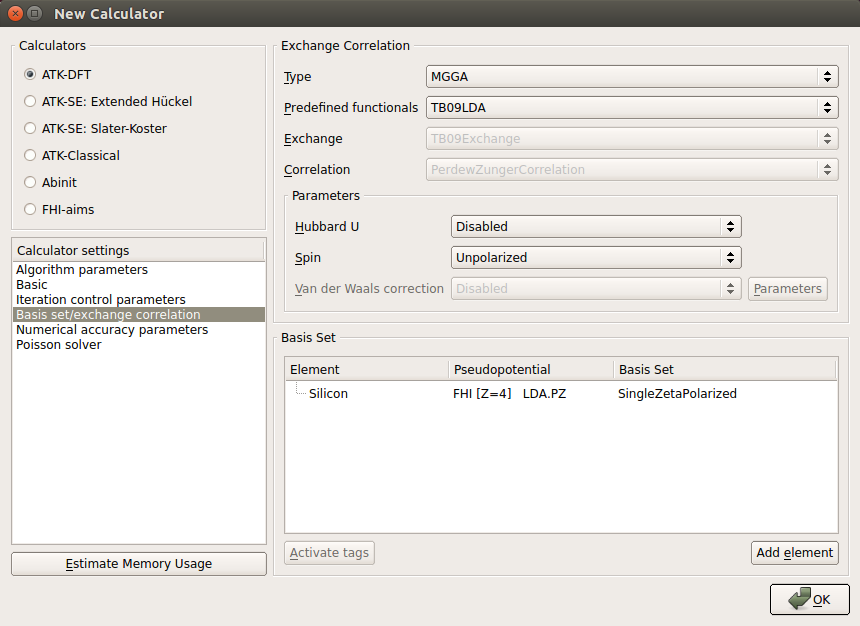
and add a New Calculator to the script. Then edit the calculator parameters:Select ATK-DFT and the MGGA exchange-correlation functional.
Use a 25x25x5 k-point sampling.
Select the SingleZetaPolarized basis set in order to speed up calculations.
Add also a
Bandstructure analysis object and set it up as you did for the Slater-Koster calculation.Back in the
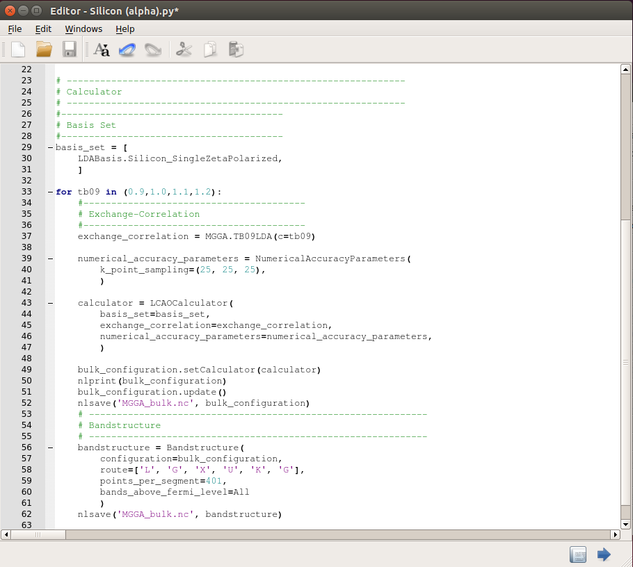
Script Generator, set the output filename to MGGA_bulk.hdf5.In order to fit the c parameter to the Slater-Koster band gap you will need to run a few calculations for different c parameters and make a linear interpolation. Here, you will run four TB09-MGGA calculations for c = 0.9, 1.0, 1.1 and 1.2. A little manual editing of the script is needed:
Send the script to the
 Editor using the button, and modify the exchange-correlation section as shown in the image below. Also, add a loop over the c values to run the four calculations with a single Python script (you can download a copy of the script here:
 MGGA_bulk.py):
Send the script to the
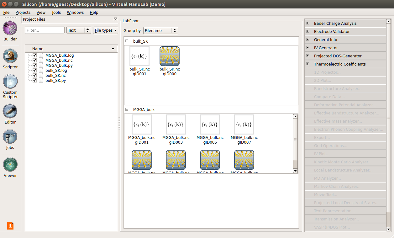
Job Manager and run the job.On the LabFloor you will now have four different Bandstructure objects included in the “MGGA_bulk.hdf5”.
You will use the following script to fit the c-parameter:
bandstructure_fit.py. Save it in the project directory.Execute the fitting script using the
Job Manager. The plot shown below should pop up.
It is clear that the TB09 c-parameter has a significant influence on the calculated band gap, and that the dependence is quite linear. The fitted value of c is 1.048.
Note
If you take a closer look at the script bandstructure_fit.py,
You will see that band gaps are calculated from a Bandstructure object like this:
bandstructure = nlread("file.hdf5", Bandstructure)[0]
gap_direct   = bandstructure.directBandGap().inUnitsOf(eV)
gap_indirect = bandstructure.indirectBandGap().inUnitsOf(eV)
print "direct gap:   %.2f eV" % gap_direct
print "indirect gap: %.2f eV" % gap_indirect
Silicon device
You will now set up the silicon device.
Open the
Builder, highlight “Silicon (alpha)” in the Stash, and start creating a Si(100) surface:Navigate to .
In the Surface (Cleave) window, choose the [1,0,0] Miller indices and click “Next”.

Keep the 1\(\times\)1 surface unit cell and click “Next”.

Select a thickness of 52 layers and click “Finish”.

Note
The 52 layers will constitute the central region of your device. You need such a relatively long device (~14 nm) because of the long screening length in the silicon semiconductor, as explained in the NiSi2–Si interface tutorial. Still, as you will see later, this device is not long enough to have perfectly converged results. However, you will use the 52 layers device throughout this tutorial to be able to perform the TB09-MGGA calculations faster.
Your Si(100) configuration is now constructed, and you will use it to construct a device with the transport direction along (100). Navigate to , keep the default parameters, and simply click “OK”.

It will prove convenient to assign tags to atoms in the regions that should be doped p-type and n-type, respectively.
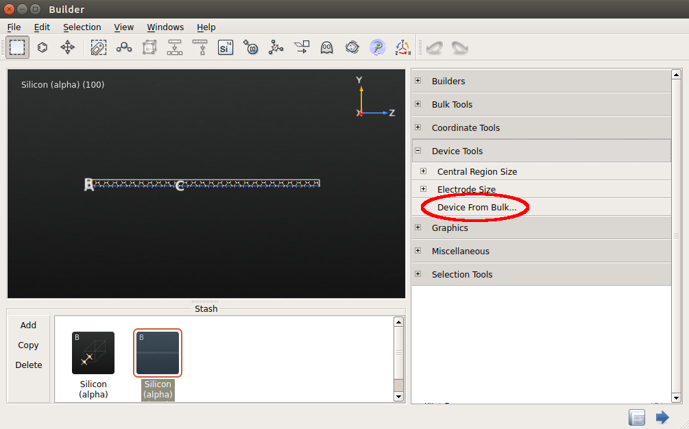
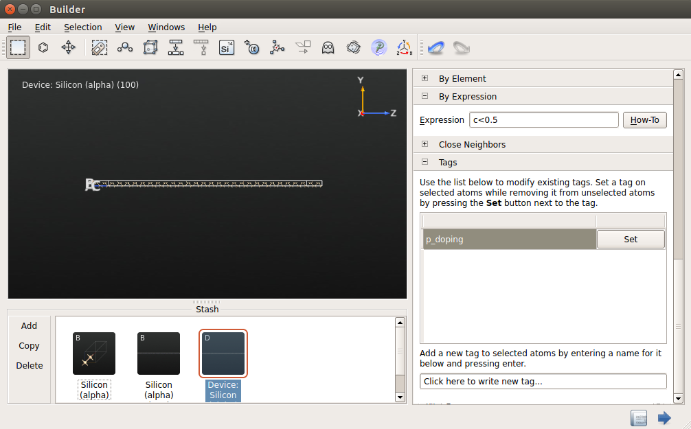
Highlight the device configuration in the Stash and go to .
Type in c < 0.5 and press Enter to select all atoms in the left hand side of the device.
Use to assign the tag “p_doping” to the selected atoms.
Follow the same procedure to select atoms with c > 0.5 and assign the tag “n_doping” to those atoms.

Slater-Koster IV curve
You will use the Slater-Koster model to calculate the I-V characteristics for the p-n doped silicon junction.
Send the device configuration from the
Builder to the Script Generator.Add a
New Calculator to the script and set the following parameters:Select the ATK-SE Slater-Koster calculator.
Use a 7x7x100 k-point sampling.
Select the Bassani.Si basis set and uncheck the “No SCF iteration” box.
You can now add all the analysis objects needed. Add the following ones:
- ElectronDensity
- DeviceDensityofStates
- ElectrostaticDifferencePotentials
- IVCurve
Edit the
DeviceDensityofStates parameters:Increase considerably the k-point sampling. Use a 21x21 grid.
Energy: from -2 to 2 eV with 401 points.
Edit the
IVCurve parameters:Voltage Bias: sample from -1 V to 1 V with 21 points.
Energy: from -1.1 eV to 1.1 eV with 401 points.
k-point sampling: 21x21.
Note
A full explanation of all the parameters is given in the Doping in QuantumATK: the Ni silicide - :ref:`nisi2-si and in the ATK Reference Manual.
Change the output filename to something like
IV_2e19_SK.hdf5.
Doping the silicon junction
You need to set up the proper doping to finally have a p-n junction. To this end, send the script to the Editor and locate the part of the script that defines the device configuration:
device_configuration = DeviceConfiguration(
central_region,
[left_electrode, right_electrode]
)
Just before those lines, add the following lines to define a p-n junction with a doping concentration of 2\(\cdot\)1019 cm-3:
# -------------------------------------------------------------
# Add Doping
# -------------------------------------------------------------
doping_density = 2e+19
# Calculate the volume  and convert it to cm^-3
# Note: right and left electrodes have the same volume,
volume = right_electrode_lattice.unitCellVolume()
volume = float(volume/(0.01*Meter)**3)
# Calculate charge per atom
doping = doping_density * volume / len(right_electrode_elements)
# Add p- and n-type doping to the central region
external_potential = AtomicCompensationCharge([
     ('p_doping', -1*doping), ('n_doping',doping)
     ])
central_region.setExternalPotential(external_potential)
# Add doping to left and right electrodes
left_electrode.setExternalPotential(
   AtomicCompensationCharge([(Silicon, -1*doping)]))
right_electrode.setExternalPotential(
   AtomicCompensationCharge([(Silicon, doping)]))
Running the calculation
Send the script to the Job Manager and run the calculation.
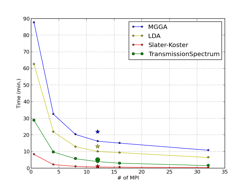
Depending on the analysis objects included in the script, and on the number og parallel processes executed by the Job Manager, the calculation may take a few minutes for the zero bias part and up to few hours to calculate the whole IV curve. The performance of ATK 2014 for different methods (ATK-SE and ATK-DFT) and for a transmission spectrum calculation are reported in the figure below.
Note
The calculations are run in parallel on different Intel Xeon e5472 3.0 GHz machines. The single points at 12 MPI are run with QuantumATK 13.8. Overall, QuantumATK 2014 is 25-30% faster compared to QuantumATK 13.8.
Calculation details: zero-bias, 7x7x100 k-point sampling for SCF part and 21x21 for the transmission spectra. All other parameters are set as in this tutorial.
Note that the Slater-Koster SCF calculation is much faster than the post-SCF calculation of the transmission spectrum.
DFT-MGGA IV curve
While the Slater-Koster job is running you can set up the DFT-MGGA calculation.
Simply go back to the Script Generator and change the Calculator block:
Choose ATK-DFT.
Exchange correlation: MGGA.
SingleZetaPolarized basis set.
Remove all analysis objects except the IVCurve. Then set up the device doping and run the calculation.
Analyzing the results
IV Curve
Once the two calculations are done and you have the output nc files in the project directory you will see the two IVCurve objects loaded in the LabFloor:
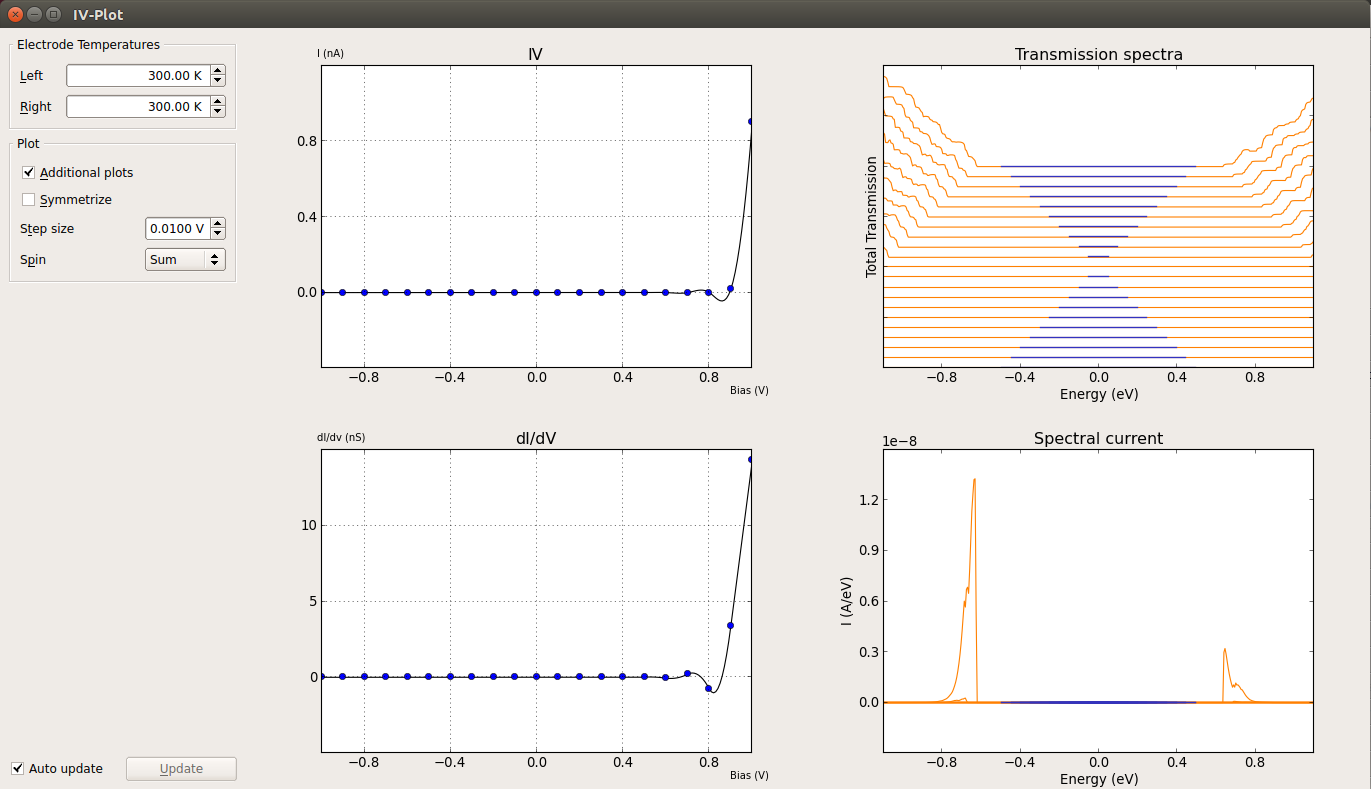
Select one of the IVCurve objects and use the IV-Plot plugin to plot the IV curve. If you check the Additional plots option, you will also see plots of dI/dV, transmission spectra, and the spectral current.
In order to compare the Slater-Koster and MGGA IV curves, and send the script to the
Job Manager to create the figure below, where you can compare directly the two IV curves. You can also open the script with the Editor and modify it to tune the plot to your best convenience.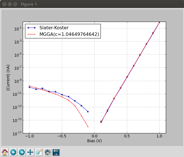
Attention
From the plot above you can see that the results from the semiempirical Slater-Koster model and the DFT-MGGA method are virtually the same.
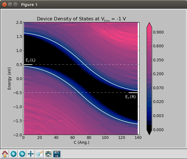
Device Density of States
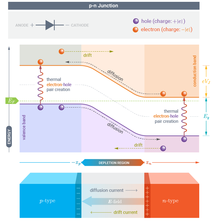
A classical picture of the electronic structure of a p-n junction is the one reported below, where the potential energy is plotted as a function of position along the transport direction of the device.
Using QuantumATK and ATK it is possible to perform this analysis through the DeviceDensityOfStates or the LocalDensityOfStates analysis objects.
Attention
Here, you will analyze the DeviceDensityOfStates and plot it along the device transport direction using a script.
In order to run the script and make the plots shown below you need an .hdf5 file containing the analysis objects DeviceConfiguration, DeviceDensityOfStates
and ElectrostaticDifferencePotential. You can open the script with the Editor and customize the plot according to your wish.
In particular, the ddos_edp.py script will read:
DeviceConfiguration: to determine the spatial resolution along the device by defining a projection list used to plot the DDOS. Also, the electrode voltages are extracted from this object.
DeviceDensityOfStates: besides reading and plotting the projected density of states, this object is also used to exctract the band edges at the left electrode. These informations are printed and used to align the electrostatic difference potential plots.
ElectrostaticDifferencePotential: to plot the average electrostatic difference potential across the device.
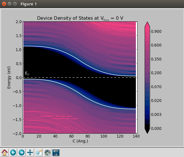
In order to get the DeviceDensityOfStates plot without an applied bias, run the script from a terminal:
atkpython ddos_edp.py IV_2e19_SK.hdf5
where IV_2e19_SK.hdf5 contains the analysis objects described above. You can also create plots for finite bias. See the section Finite-bias calculations. Results are illustrated below.
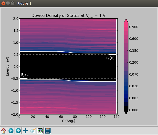
Finite-bias calculations
In order to create the finite-bias plots (Vbias = -1 and 1 V), do as follows:
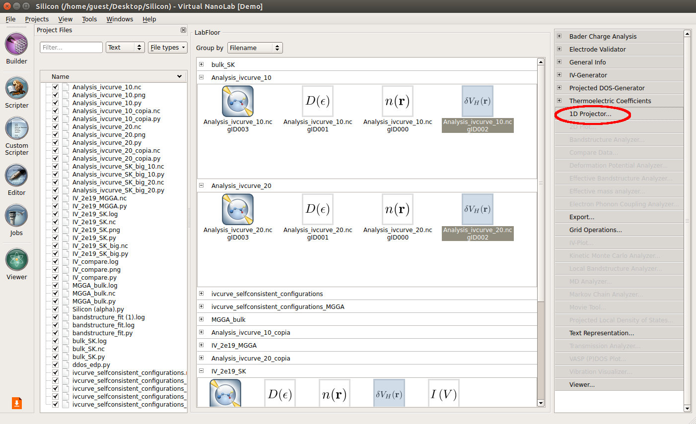
Go to the Labfloor and from the
ivcurve_selftconsistent_configuration.hdf5file select the device configuration obtained at Vbias = -1 V, and drag and drop it onto the Scripter. The following window will show up.
Remove the
New Calculator object and add instead  Analysis from File.
In
Analysis from File, set the HDF5 file and the Object id of the device configuration object.
Then, add the Electrondensity, DeviceDensityOfStates and ElectrostaticDifferencePotential analysis objects and set the parameters as described above.
Change the output file to
Analysis_ivcurve_10.hdf5.Before running the job, send the script to the
Editor, and add the following line to get the device_configuration file within the Analysis_ivcurve_10.hdf5output file.# ------------------------------------------------------------- # Analysis from File # ------------------------------------------------------------- device_configuration = nlread('ivcurve_selfconsistent_configurations.hdf5', object_id='ivcurve010')[0]
After this part and just before ElectronDensity, add the following line:
nlsave('ivcurve_selfconsistent_configurations.hdf5', device_configuration)
Lastly, save the script and run the job. Once the job have finished, run the script
ddos_edp.pyin order to get the Device Density of States plot. Run the script as follows:atkpython ddos_edp.py Analysis_ivcurve_10.hdf5
You can plot the Device Density of States plot following the same procedure for the ivcurve_selftconsistent_configuration.hdf5ivcurve020 file.
Electrostatic potential

In the Labfloor, select the ElectrostaticDifferencePotential objects obtained for Vbias = 0, -1, 1,
Use the 1D Projector plugin to plot the data.
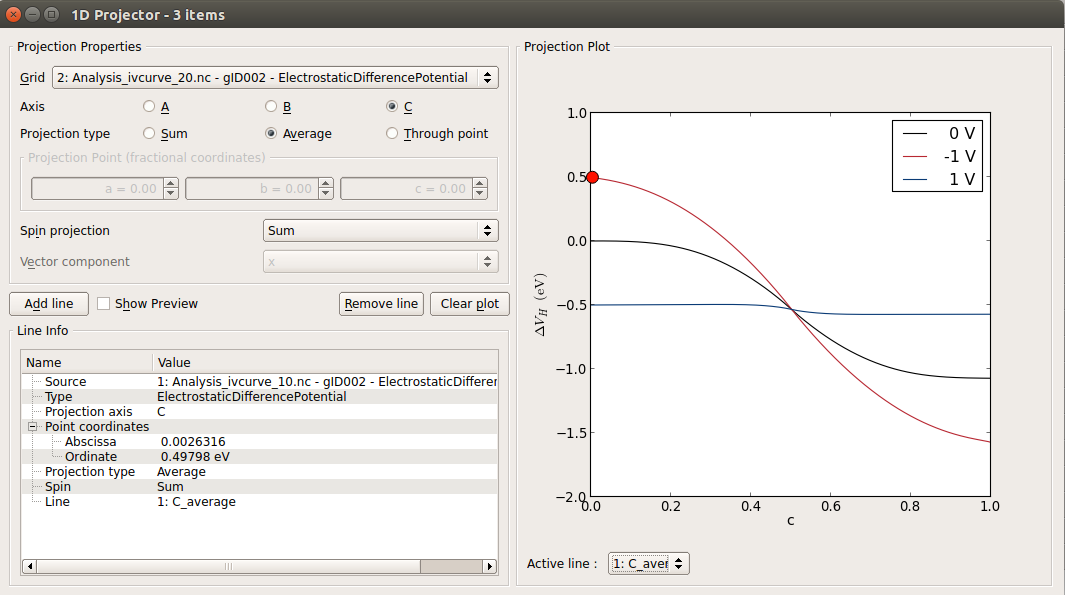
You can see that the results are not perfectly converged wrt. the length of the device, because the gradient of the electrostatic potential is not zero at the ends of the device central region. The figure below compares the ElectrostaticDifferencePotential of the device used in this tutorial with results for a longer one.
