Opening a band gap in silicene and bilayer graphene with an electric field
Version: 2017
In this tutorial you will learn how to insert metallic gate electrodes in an QuantumATK bulk calculation and use them to apply electric fields. You will use these features to study the opening of a band gap in bilayer graphene and in silicene under the presence of an electric field. It is assumed that you are familiar with the basic functionalities of QuantumATK.
Bilayer graphene
Building a bilayer graphene structure
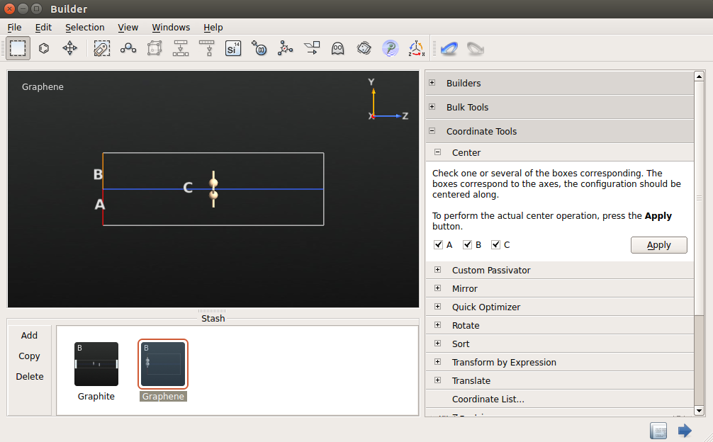
Create a new empty project and open Builder (icon
 ).
).Insert graphite (not graphene!) from Database.
Open . Select Cartesian coordinates and set the value of c lattice constant to be 25 Å.
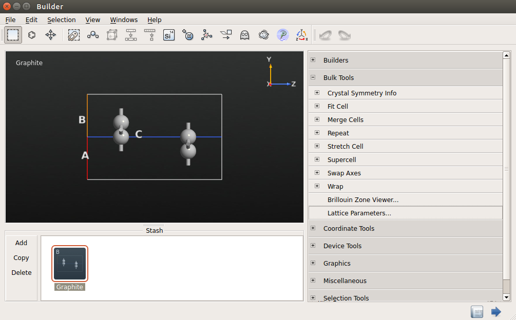

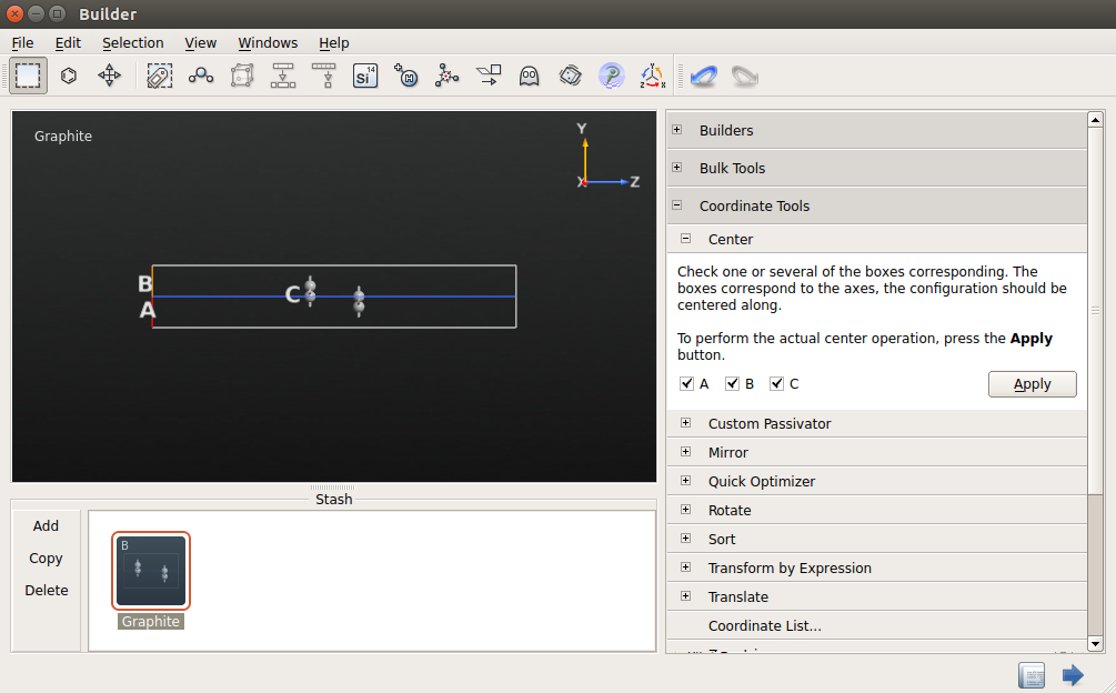
Go to and click “Appy” to center the system.
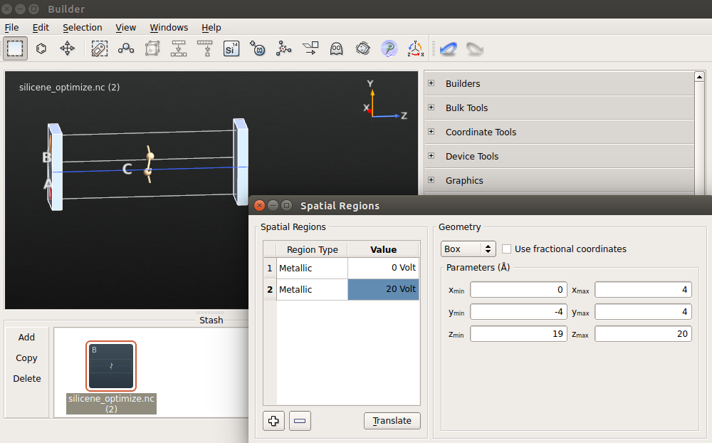
To insert the metal electrodes, open , right-click the table (the area under the headers Region Type/Value) and click “Insert region” twice.
Set the voltage to 0 V for the first metallic region, and 10 V for the second. Change their size so that they cover the entire hexagonal unit cell (see the figure below). It does not matter if the regions stick outside the cell, those parts will be ignored in the calculation anyway.
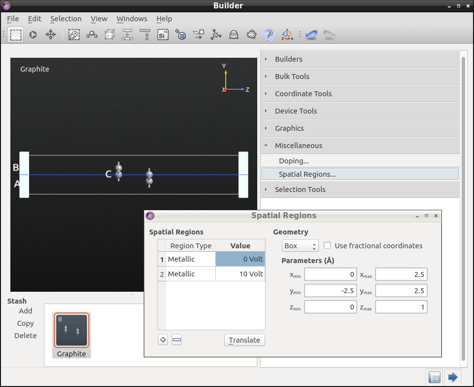
The applied voltage results in 4 V/nm in the z direction, just above the field that has been found in experiments to open a band gap.
Calculation and analysis
We will then analyze the band structure of the graphene bilayer under the static electric field.
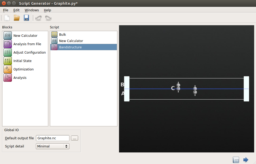
Send the graphene bilayer structure to Script Generator.
Insert a New Calculator block
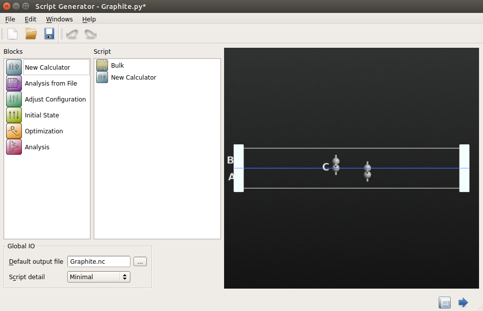
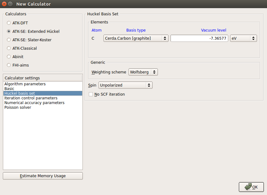
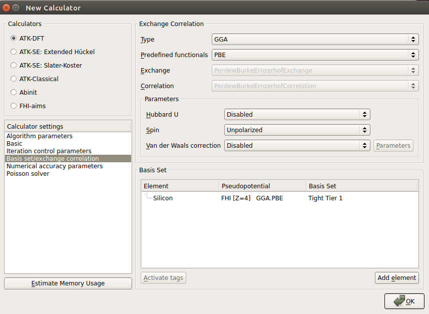
Open the New Calculator block, and choose the “ATK-SE: Extended Hückel” method. For good accuracy, set the k-points to be 9x9x1.
Under “Huckel basis set” select the “Cerda. Carbon [graphite]” basis set, which describes the sp2 bonding of graphene very well.
Untick the “No SCF iteration” option to carry out the computation self-consistently.
Warning
It is extremely important to include self-selconsistency; otherwise the field will not have any effect at all!
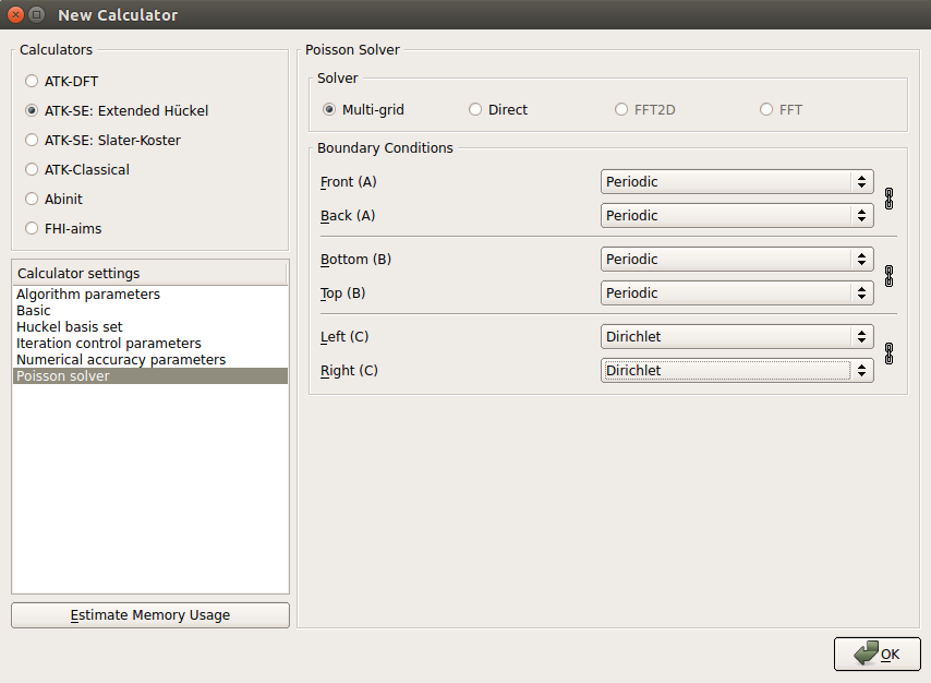
Go to “Poisson solver”, set “Multi-grid” in Solver, and choose “Dirichlet” in Boundary Conditioins on both sides in the C direction.
Note
For this particular calculation, you can choose any boundary condition in the C direction since the metal gates will fix the potential at the boundaries anyway, but “Dirichlet” is the physically correct condition when a constant value of the potential is desired at the boundary.
Add a Bandstructure block by clicking .
Double-click the Bandstructure block and change the route to G, M, K, G. Also increase the number of points per segment to 200.
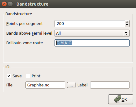
Name the output file “bilayer_graphene_efield.nc”.
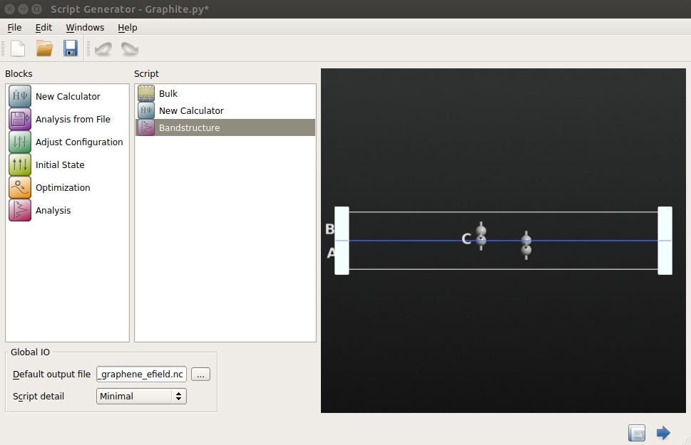
Send the calculation to Job Manager, save the Python script in the window that appears and run the calculation. It should take no more than 20-30 seconds to run.
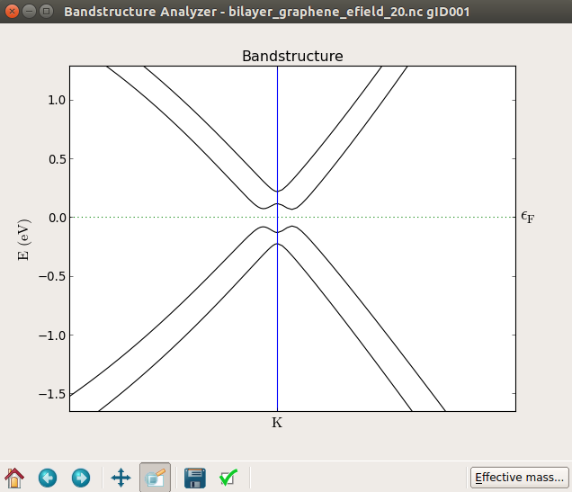
After the calculation, visualize the band structure and zoom in around the K point, where a band gap is opening with increasing the strength of the electric field. The following figures, from top to bottom, show the band structure of the bilayer graphene with an applied electric field of 0, 10, and 20 Volts, respectively.


Note
You can use DFT as well, the results will be similar.
No attention was paid to the interlayer distance. You can change it a bit to see how the band structure changes. Note, however, that you cannot use DFT/GGA to optimize this distance because no energy minimum will be found, due to the absence of dispersion corrections (the layers are bound by Van der Waals forces, not captured in standard GGA). LDA works, fortuitously, because of a cancellation of errors, but the results cannot really be trusted.
Silicene
To study the effect of electric fields on silicene you first need a good model of this material. The approach will be to start with graphene and turn it into silicene, optimize the geometry, and then repeat the same steps followed to calculate the bilayer graphene under the presence of an electric field.
Optimizing the geometry
In Builder, add graphene (not graphite this time) from Database to Stash following the same steps explained above for the bilayer graphene.
Change the two C atoms to Si by selecting them (using the left mouse button while holding down the
Ctrlbutton of your keyboard) and using the “Periodic Table” tool .
.The lattice constant of silicene is not the same as for graphene, but rather than guess it, it will simply be part of the geometry optimization to determine it. To start from a reasonable guess, click . Make sure to keep the fractional coordinates constant, set the lattice parameter a to be 3.8 Å and increase the c lattice parameter to 20 Å.
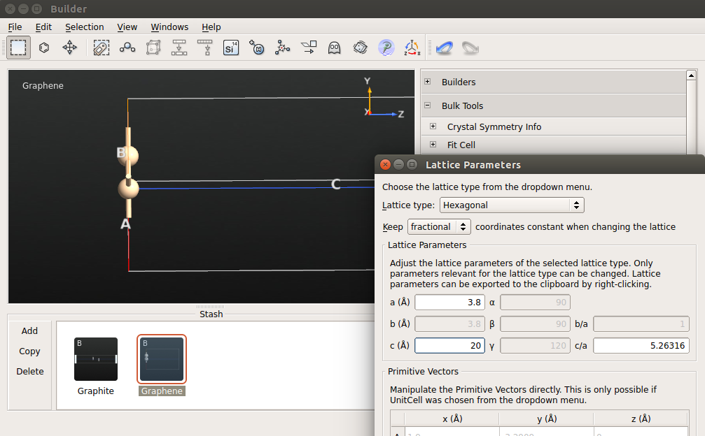
In Builder, go to , in order to center the configuration.
The flat geometry where both Si atoms are in the same plane is a local minimum in the potential energy surface. Therefore, click the “Rattle” tool
 a few
times to add a small perturbation to the coordinates. This ensures that the geometry
optimization will converge to the global minimum.
a few
times to add a small perturbation to the coordinates. This ensures that the geometry
optimization will converge to the global minimum.Send the geometry to Script Generator by using the “Send To” button
 .
.In Script Generator, insert New Calculator and OptimizeGeometry blocks by double-clicking the icons in the Blocks panel:
 New Calculator.
 .
.
Use 21x21x1 k-points for good accuracy, and choose GGA-PBE for exchange-correlation. You can in principle use the default DoubleZetaPolarized basis set, but here you will use the “Tight Tier 1” basis set, which provides slightly better results.
In the OptimizeGeometry block, set the force tolerance to be small (0.01 eV/Å) and the stress tolerance to be even smaller (0.0005 eV/Å3). Unconstrain the cell in the x and y directions.
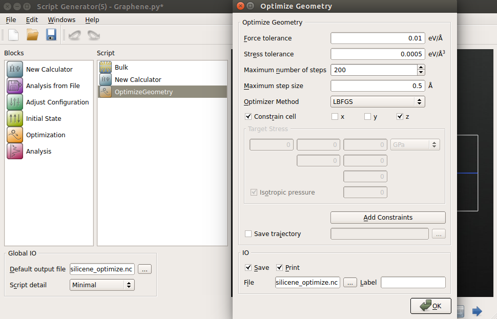
Name the output file “silicene_optimize.nc” and save the Python script.
Send the script to Job Manager, save the script and run the job. The calculation will take about 10 minutes. When it finishes, drop the Bulk Configuration with ID “gID001” on Builder, and inspect the geometry. You will find a nicely optimized silicene sheet with a buckling of about 0.5 Å and an optimized lattice constant of 3.86 Å. Both values are in good agreement with those reported in the literature in [1] and [2].
Band structure
Using the optimized structure, repeat the steps above for the bilayer graphene to insert metallic gates and compute the band structure with electric fields. Notice that, in the case of silicene, you need to make the spatial region larger in the XY plane, since the cell is also larger. Use 20 V as the voltage on the second electrode.
Note
You should use the same calculator settings as for the optimization. The calculation will take less than a minute.
In the plot below you can see the band structure at zero field (top) and with 20 V applied on the gate (bottom), which produces a band gap of about 0.1 eV. By trying different values of the voltage you will find that the band gap increases essentially linearly with the field as shown in [3].
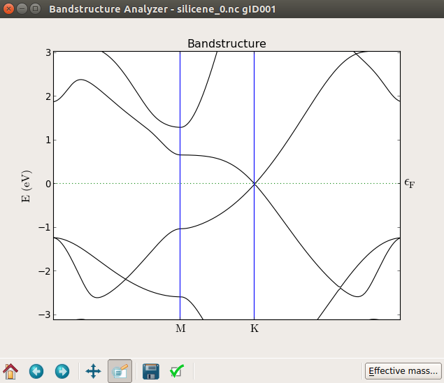
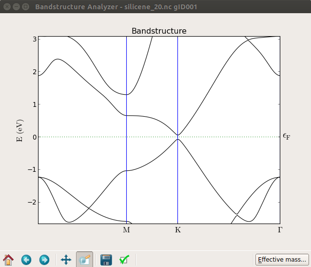
Notice that in this case, if you look closely, the band gap is not exactly at the K point.
Note
If you apply a transverse field to a single graphene layer, no gap opens up. The reason is that the graphene is completely flat, and so the field just gives a constant shift of the potential. In the case of silicene the gap appears because the sheet is naturally buckled.
References
More reading
For a similar study on hexagonal boron-nitride (hBN), see