Modeling Schottky barrier heights: The Ag–Si interface
Version: X-2025.06-SP1
The Schottky barrier is the energy barrier that forms at the interface between a metal and a semiconductor, determining how easily electrons can cross the junction. It strongly influences current flow in Schottky diodes and metal-semiconductor devices, thereby affecting key performance factors such as switching speed, leakage current, and efficiency in electronic components like rectifiers, transistors, and solar cells.
In this case study, we will use QuantumATK to calculate the Schottky barrier height for a Ag-Si interface, following the methodology reported in the publication “General atomistic approach for modeling metal–semiconductor interfaces using density functional theory and non-equilibrium Green’s function” [1]. While Ag–Si is treated here as a representative case, the same approaches can be applied to any metal-semiconductor interface.
You will see that determining the Schottky barrier height is not always straightforward, since many physical and computational factors influence its value. To illustrate this, we will explore several complementary approaches based on density functional theory (DFT) and the non-equilibrium Green’s function (NEGF) formalism.
You will be guided through the following steps:
Creating the device and relaxing it
Calculating the Schottky barrier height using the Hartree difference potential
Calculating the Schottky barrier height using the projected local density of states
Calculating the ideality factor
Estimating and analyzing the Schottky barrier from the activation energy
Calculating the spectral current to determine the transmission channel
Note
This tutorial is intended for advanced users of QuantumATK. The instructions are deliberately concise to focus on the scientific concepts and workflows, assuming familiarity with the software.

Creating the device
Tip
If you wish to skip this part, you can just download the optimized device configuration
as a QuantumATK Python script: relaxed_device.py.
The first step is to relax the bulk structures of silver and silicon. Build the
structures using the database in the  Builder and send them both
to the
Builder and send them both
to the  Workflows, one at a time. In both scripts, add a
 Set LCAOCalculator block with the following settings:
LDA exchange-correlation functional
FHI Pseudopotential
DoubleZetaPolarized basis set
Broadening 300 K
11x11x11 k-point sampling
Also add the  OptimizeGeometry block, set the force and
stress tolerances to 0.01 eV/Å and 0.001 eV/Å3, respectively. Run both scripts to obtain the optimized structures.
The calculations can easily be run on your local machine.
OptimizeGeometry block, set the force and
stress tolerances to 0.01 eV/Å and 0.001 eV/Å3, respectively. Run both scripts to obtain the optimized structures.
The calculations can easily be run on your local machine.
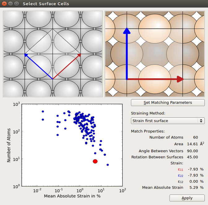
The Ag and Si (100) surfaces can now be created by using the Surface (Cleave) tool in the Builder, and from these you can create the interface using the Interface builder tool. You should include 6 layers of Ag and 9 layers of Si. Choose Strain first surface in the Select Surface Cells window under Straining method and choose the cell shown in the figure below.
In the Shift Surfaces Cells set the displace in the z-direction to 2 Å and click apply. This will displace the entire Si side, such that there is 2 Å between the two surfaces. Finally, click Create.
Tip
You can learn more about the Interface Builder in the Technical Notes on it: Interface Builder.
Verifying atomic site alignment at the interface
Use the Repeat tool to repeat the interface 2 times along the B-direction. The interface builder initially lines up the surfaces at a hollow site. We know from the paper [1] that this is the most stable conformation, so make sure this is the case and if not, use the  Move tool to fix it.

Note
Repeating the structure is not required for the simulation itself. In this tutorial, we repeat it to visually reproduce the structural model used in [1], which helps clarify the alignment of atomic sites at the interface.
Device setup and relaxation
When utilizing the interface builder, the silver electrode experiences strain along both the x- and y-directions. For a more accurate representation of the electrode’s mechanical response, relaxation in the z-direction should also be considered, in accordance with the material’s Poisson ratio. This adjustment is not automatically performed by the OptimizeDeviceConfiguration function which we will use later and must therefore be implemented manually, before optimizing the final device.
Use the Device From Bulk plugin to turn the bulk into a device, just use the default settings and press Ok. Now use the  Split button to split the Ag electrode from the device and send it to the workflow. Use the same optimization setup as for the bulk optimization but change:
K-point sampling to 6x3x1
In the OptimizeGeometry module constrain the cell in x and y but not z, to let the z direction relax accordingly.
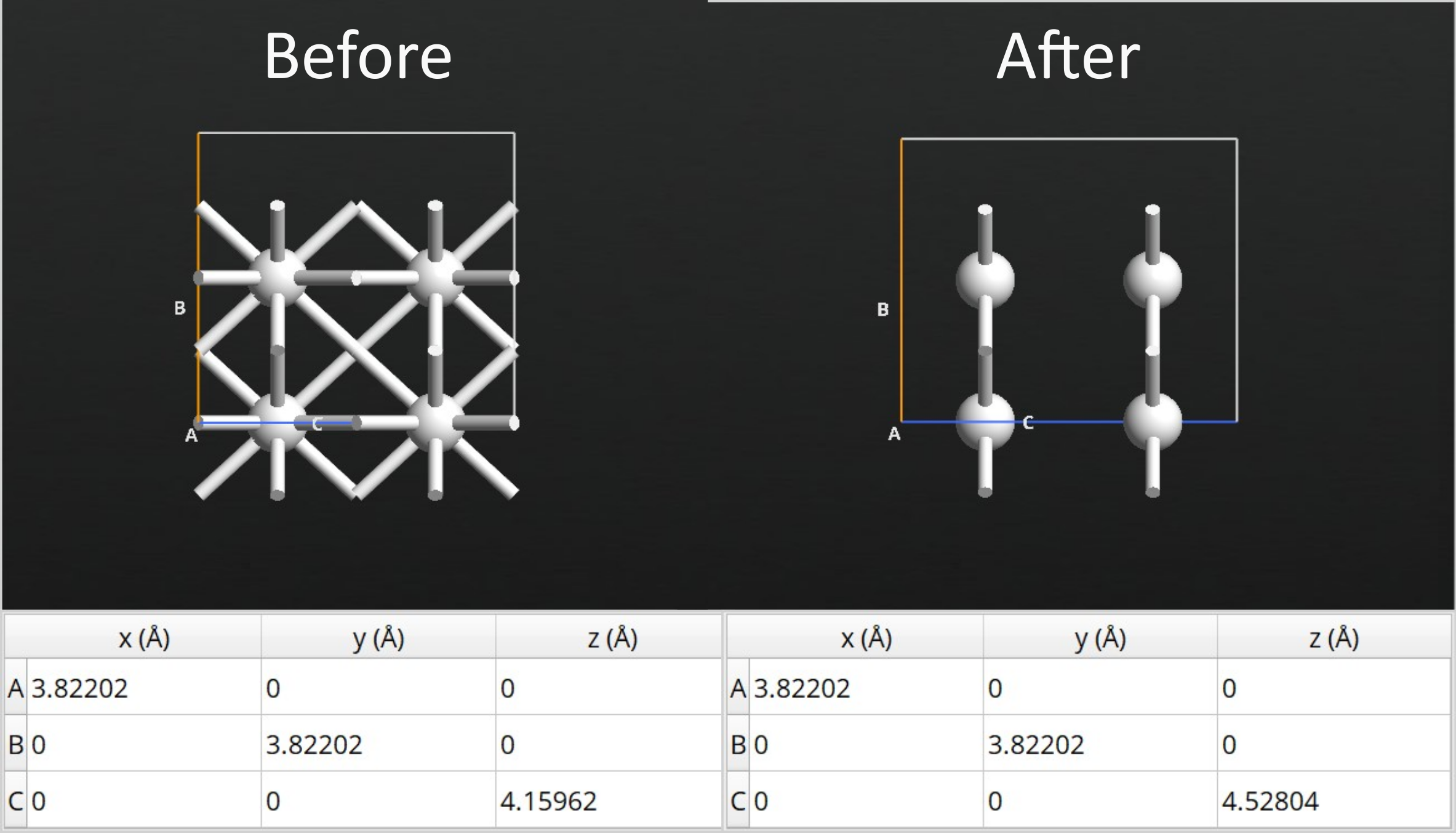
After running the relaxation, you will find that the length of the electrode C-vector increases by 8.82%. To be consistent, you should apply the same elongation to the Ag part of the interface configuration.
Use the Stretch Cell tool:
Select all the Ag atoms
enter 1.0882 for the stretch along C and choose Selected atoms are stretched
Now the final device can be built, again using the Device From Bulk plugin. This time, add layers of both surfaces to the central region such that there is 12 silver and 36 silicon layers. To relax the device, set up a workflow with a Set DeviceLCAOCalculator with the following parameters:
LDA exchange-correlation functional
FHI Pseudopotential
DoubleZetaPolarized basis set
Broadening 300 K
6x3x401 k-point sampling
Add the  OptimizeDeviceConfiguration from
  Studies category and set the Maximum force tolerance to 0.02 eV/Å and passivate only the right side. You can read more on the manual page: OptimizeDeviceConfiguration. The calculation takes about 40 minutes using a single node with 40 CPU cores. If you do not intend to run
the calculation, you can download the relaxed device configuration here:
Studies category and set the Maximum force tolerance to 0.02 eV/Å and passivate only the right side. You can read more on the manual page: OptimizeDeviceConfiguration. The calculation takes about 40 minutes using a single node with 40 CPU cores. If you do not intend to run
the calculation, you can download the relaxed device configuration here:
relaxed_device.py. You can also download the workflow device-optimize_WF.hdf5 and the results device-optimize_results.hdf5.
Fitting the TB09-MGGA c-parameter
Standard DFT functionals like LDA and GGA are known to systematically underestimate band gaps, especially in semiconductors. This limitation can significantly affect the accuracy of transport simulations, particularly when modeling interfaces where band alignment plays a crucial role. To overcome this, we employ the Tran-Blaha meta-GGA (TB09) functional [2], which introduces a tunable c-parameter, allowing for improved band gap predictions. The c-parameter must be carefully fitted to reproduce the experimental band gaps, ensuring a more realistic description of the electronic structure on the semiconductor side of a device.
In order to obtain an accurate description of the Si side of our interface, the TB09 c-parameter is fitted to match the silicon band gap. Details about this procedure can be found in the tutorial Meta-GGA and 2D confined InAs. The calculations are quite fast and can be run locally.
Follow these steps:
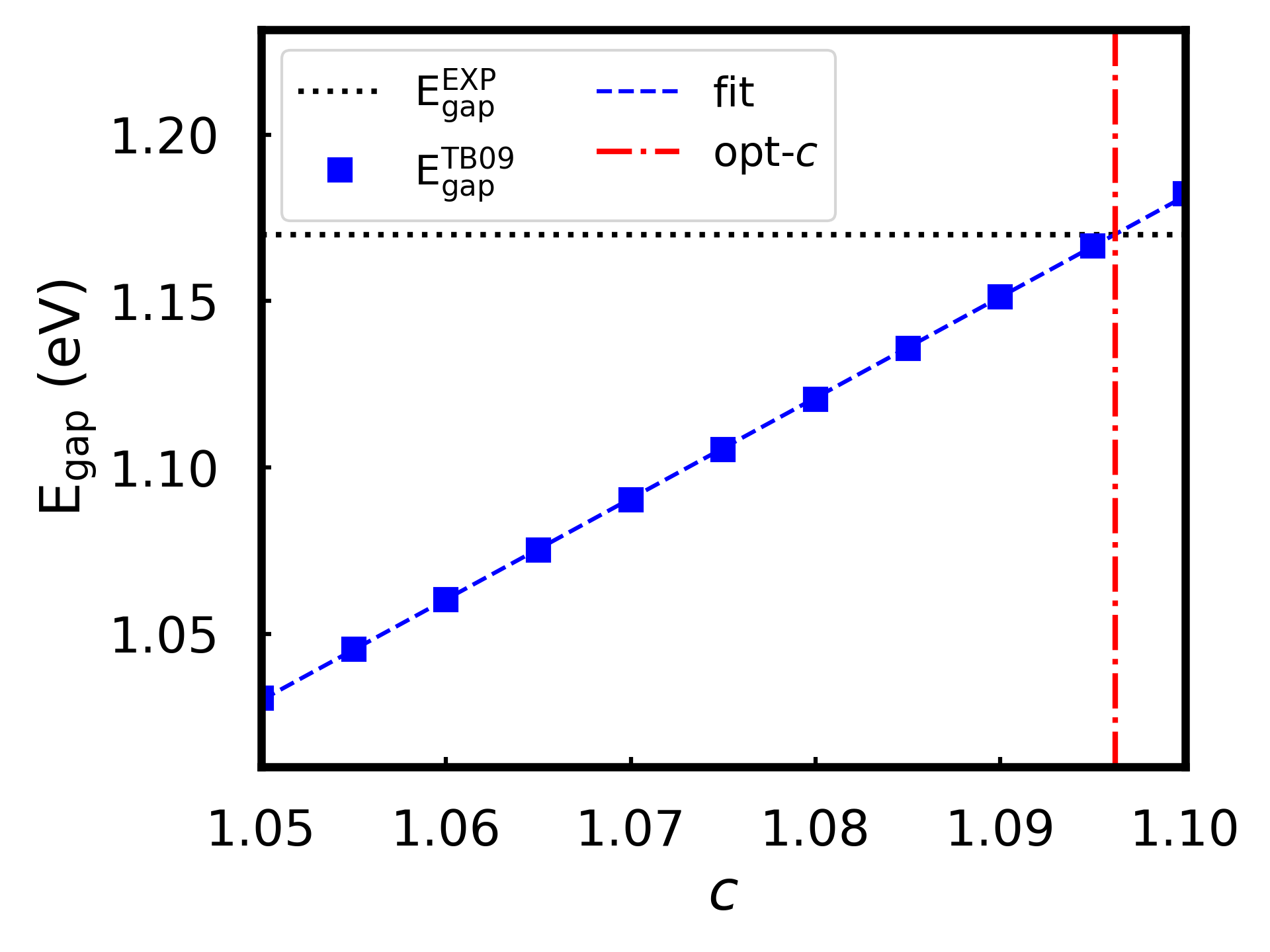
Compute the band structure of the optimized silicon bulk (before cleaving it) using LDA exchange correlation and FHI pseudopotential with the TB09-MGGA functional and 11x11x11 k-points. You should obtain a band gap of 1.17 eV and a self-consistently determined c-parameter of 1.0842.
Do similar calculations as before. This is easiest done by copying the workflow and changing the name. This time we will fix the c-values around 1.0842. This can be done in a single QuantumATK Python script by looping over the different c-values. In the LCAO calculator where you set the functional, press Advanced Parameters and untick the self-consistent box. Send
 the workflow to
  Editor and locate the Exchange-Correlation section and insert the loop:
10# %% Set LCAOCalculator
11
12# %% LCAOCalculator
13
14for tb09 in (1.05,1.055,1.06,1.065,1.07,1.075,1.08,1.085,1.09,1.095,1.1):
15    # ----------------------------------------
16    # Exchange-Correlation
17    # ----------------------------------------
18    exchange_correlation = TB09CustomExchangeCorrelation(
19    correlation=PerdewZunger,
20    c=tb09,
21    alpha=-0.012,
22    beta=1.023 * Bohr ** (1 / 2),
23    number_of_spins=1,
24    spin_orbit=False,
25    )
26
27    # ----------------------------------------
28    # Basis Set
29    # ----------------------------------------
Remember that the Bandstructure block should be included in the loop, just below the Calculator section. Use
nlsave('C2_results.hdf5', bandstructure)to save all the band structures in a single data file.Fit the c-value to the experimental band gap of 1.17 eV [3] using the script
c_fit.py. It needs three input parameters; a list of the used c-values (tb09), the name of the .hdf5 file containing the bandstructure calculations (fname), and the experimental band gap (SK).
The optimal c-value is found to be 1.0962. This c-value for the TB09 functional is applied in all following calculations.
Tip
The loop created in Scripter in step 2, can also be set up directly in the workflow by using the  Iteration block. However, this feature currently has a bug and does not work.
Zero-bias calculations
Before being able to calculate the projected density of states and the Schottky barrier, it is important to ensure that the device length exceeds the semiconductor’s screening length, so the potential at the silicon–electrode boundary matches that of bulk silicon. This can be done by studying the convergence of the Hartree potential with respect to the length of the silicon central region.
Silicon doping and depletion layer length
You are now ready to dope the silicon part of the device. Open the relaxed
device configuration in the Builder, select all the silicon
atoms, and use the Doping plugin to apply an n-type doping concentration
of 1019 e/cm3. Make sure the Unit is set to the right electrode, so it is correctly referenced to silicon.
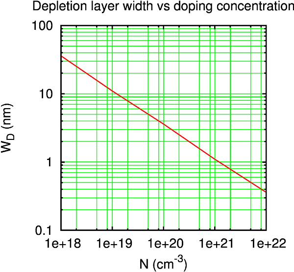
For a good starting guess of the length needed, you can consult some typical depletion layer lengths for metal–semiconductor interfaces [4]. As seen from the figure below, a doping of 1019 cm-3 corresponds to a depletion layer length of around 100 Å.
Tip
You only need to converge the length of the silicon side of the interface, since the metal has a much shorter screening length. The atomic layers of Ag we have will be sufficient.
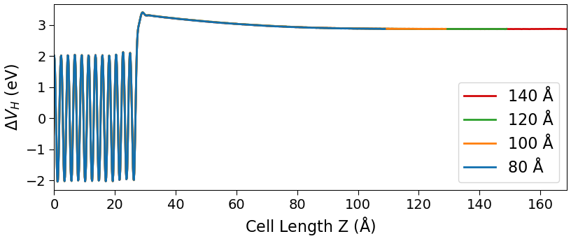
Increase the length of the silicon part of the central region by using the
Central Region Size in the panelbar. Use lengths of 80 Å, 100 Å, 120 Å, and 140 Å,
and send each device configuration to the Workflows.
Use a calculator with the same parameters as for the device relaxation, now with the TB09 functional and the c-parameter from before. Then add the  HartreeDifferencePotential block.
Note that the calculations become increasingly difficult to converge as the length is increased. At 120 Å and more, you will need to adjust the Iteration Control Settings in your calculator: In the DeviceLCAOCalculator, go to the Iteration Control and set the following parameters:
Max steps = 400
Damping factor = 0.05
Number of history steps = 12
The calculation for the largest device requires approximately 20 minutes on a single node with 40 CPU cores.
When all calculations have finished and the results appear in the  Data.
You can plot the potentials along the Z-direction using the 1D projector
analysis tool and use the
Data.
You can plot the potentials along the Z-direction using the 1D projector
analysis tool and use the  drag and drop function to combine the plots. The potential should be flat in the vicinity of the boundary
with the silicon electrode.
drag and drop function to combine the plots. The potential should be flat in the vicinity of the boundary
with the silicon electrode.
Note
When combining plots in the GUI, it’s important to add them in specific order, starting with the largest device and proceeding in decreasing size. This ensures that all plots remain visible, as the GUI layers them chronologically and does not allow reordering afterward.
We now need the macroscopic average of the potential,
\(\langle \Delta V_H \rangle\). Use the script hdp.py to calculate the macroscopic average of the Hartree potential along the z-direction [5]. The script loops over the four different devices and creates .dat files for each device containing the averaged data. It needs to be edited, as it contains some input parameters specific to the interface structure;
device_files: Names of the .hdf5 files containing the Hartree difference potential for each device
output_names: Names for the output .dat files containing the averaged potentials
names: Names for the legends on the plot
gauss_left: Distance along Z (in Å) between two consecutive atomic layers in the left electrode material
gauss_right: Same as above, but for the right electrode material
zcoord_int: Z-coordinate of the interface position (in Å) calculated as the midpoint between the last atom in the left-hand material and the first atom in the right-hand material
Once you have edited these parameters, run the script by sending the scripts to  Jobs.
Jobs.
The script also produces the figure below, which compares the four different potentials.
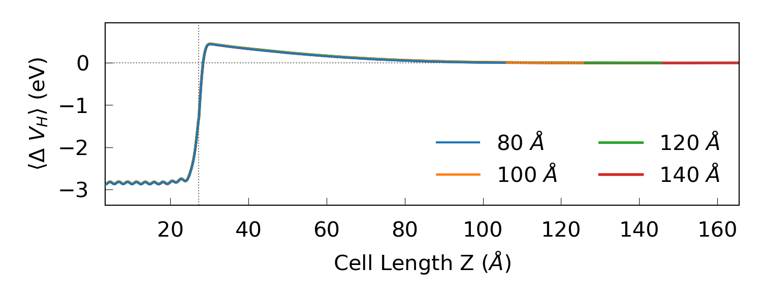
We may conclude from the plot that a silicon central region length of 120 Å
should be sufficient. Note that the depletion layer length could change
slightly with the bias. You can download the final device configuration final-device.py along with the workflow device120_WF.hdf5 and results device120_results.hdf5.
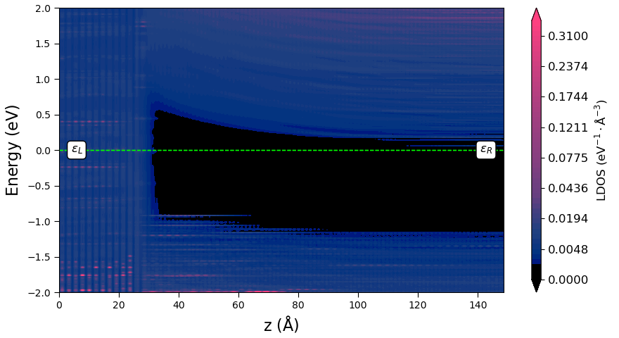
Projected local density of states
The projected LDOS (PLDOS) offers a highly useful visualization of the band diagram of the interface. Set up the workflow:
Use the
 Load from file block in the Workflows to load the saved device configuration and the converged calculator attached to it from the
 device120_results.hdf5file.Add the
ProjectedLocalDensityOfStates block and edit the settings:Energy range: -2 and +2 eV using 401 energy points
K-points: Monkhorst-Pack grid 18x9
The calculation will take less than an hour on a 40-core node. You can download the workflow PLDOS_WF.hdf5 and results PLDOS_results.hdf5. When the calculation is finished and the results can be found in Data, you can use the Projected Local Density of States analysis plugin to plot the PLDOS along the device transport direction:
You can also plot the averaged Hartree difference potential along
with the PLDOS using the script pldos_hdp.py. It requires the two .hdf5 files containing the HartreeDifferencePotential and ProjectedLocalDensityOfStates analysis items, and the same input
parameters as hdp.py, along with some plotting preferences;
fname1: Name of file containing HartreeDifferencePotential
fname2: Name of file containing ProjectedLocalDensityOfStates
leftname: Name of the left-hand interface material
rightname: Name of the right-hand interface material
lenleft: The amount of left material shown in the plot (in Å)
Run the script by sending it to Jobs, to produce the plot below:
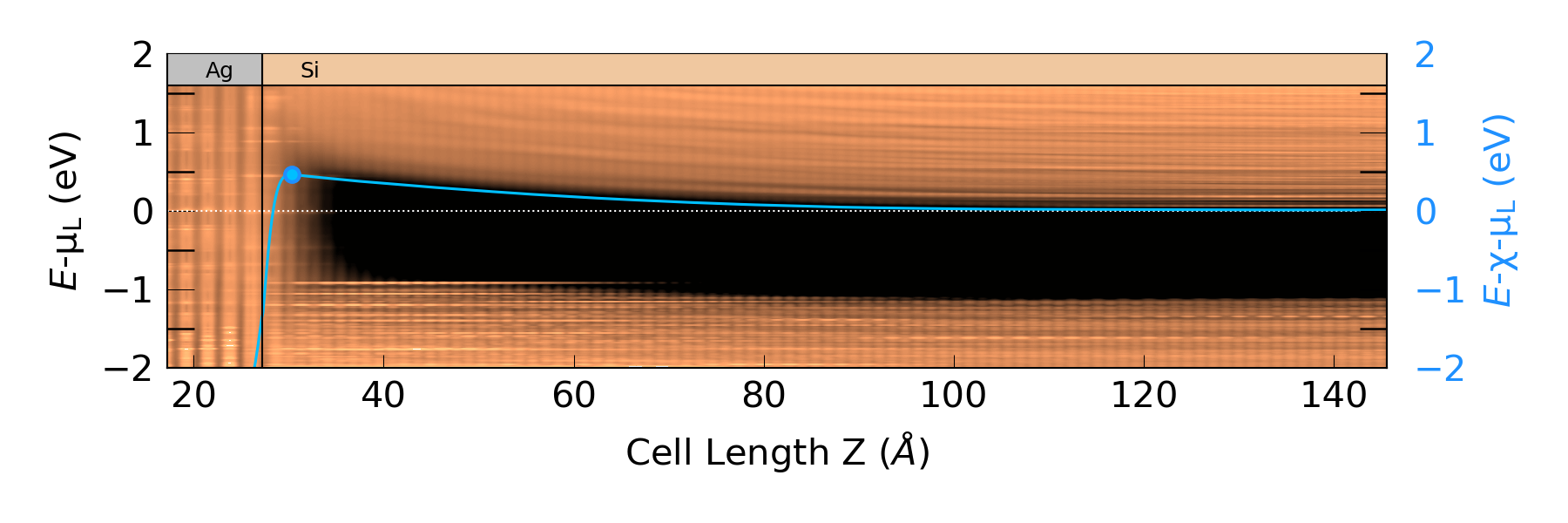
In this plot, you can easily see the metal-induced gap states to the right of the interface border. Moreover, the averaged potential nicely follows the conduction band minimum, both at the interface and far from it. We can therefore estimate the Schottky barrier, \(\Phi^{pot}\), by calculating the difference between the chemical potential of the left electrode, \(\mu_L\), and the maximum of the Hartree difference potential, \(\langle \Delta V_H \rangle\), near the interface. The plotting script returns this barrier value together with the plot and the maximum \(\langle \Delta V_H \rangle\). You will get a barrier of around 0.45 eV, which is in agreement with experimental results, see [6] and [7]. The maximum \(\langle \Delta V_H \rangle\) is 0.46 eV, which is marked on the plot. The script also returns the position of the conduction band minimum with respect to \(\mu_L\). You will need this value later on for analyzing the spectral current.
Finite-bias calculations
We will investigate the I–V characteristics next. Use the
Load from File functionality to load the device and calculator from earlier and add the  IVCharacteristics study
block. Open it and apply the following settings:
IVCharacteristics study
block. Open it and apply the following settings:
-0.3 to +0.3 V bias range with 13 points.
18x9 k-point grid.
Under Analysis click  and add HartreeDifferencePotential, this will add a Hartree difference potential calculation for each voltage in the bias range.
The calculation will require around 2 hours on a single node with 40 CPU cores. You can download the workflow IVCharacteristics_WF.hdf5 and results IVCharacteristics_results.hdf5. You can use the IV-Characteristics Analyser plugin to plot the calculated current vs. Drain-Source Voltage, or use the script IV.py to plot the current density against bias. The script requires the two .hdf5 files containing the device configuration and IVCharacteristics object.
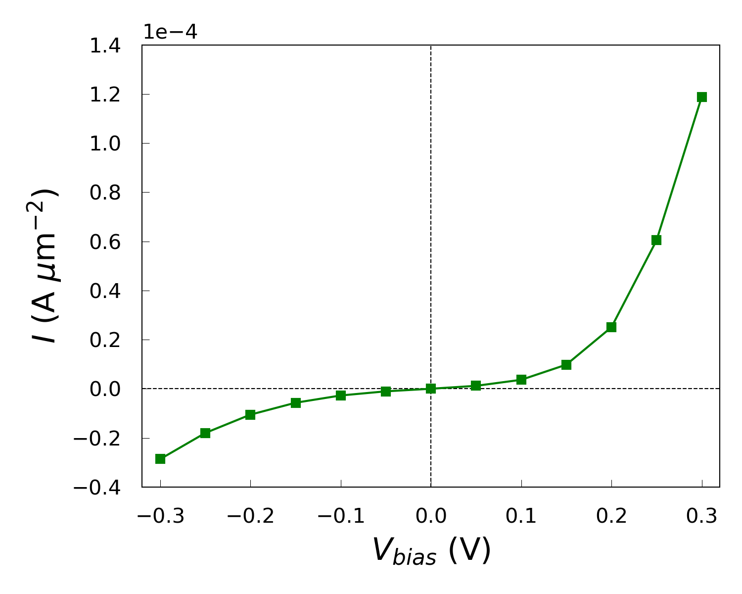
While the IV curve looks to behave as expected under forward bias, it also shows a significant current under reverse bias, indicating that the device does not exhibit ideal diode-like behavior.
Note
The computed current is significantly lower than the current reported in the publication [1]. See Appendix Note for an expanation of the variation of the current.
Reverse Bias Investigation
To investigate the current under reverse bias, we will set up some PLDOS calculations at different biases.
Again, use the Load from File functionality but here load the results file containing the IVCharacteristics.
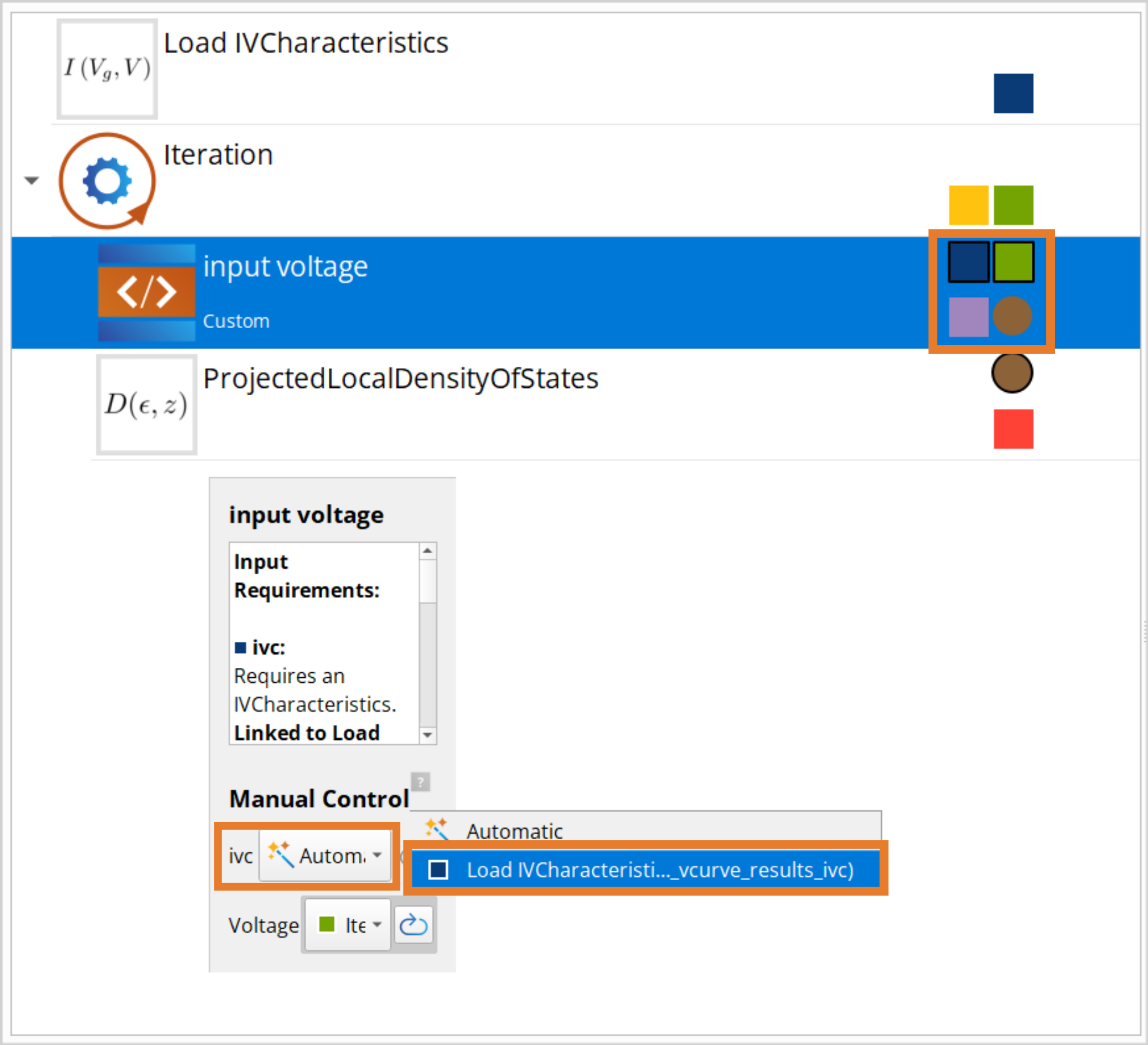
Add the following blocks to the workflow:
- Iteration
 Custom
 ProjectedLocalDensityOfStates
Make sure the Custom and ProjectedLocalDensityOfStates blocks are inside the iteration loop by dragging them onto the Iteration block.
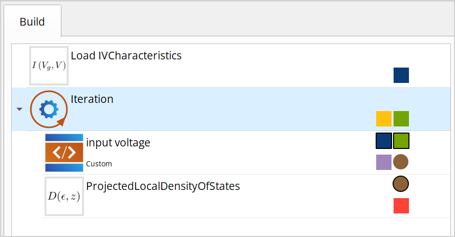
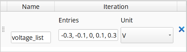
Double click the Iteration block and add a list of quantities. Name it “voltage_list”, set entries to -0.3, -0.1, 0, 0.1, 0.3 and set the unit to Volt.
Now double click the Custom block.
Under Inputs, add Type and name the variable “ivc” and set the type by writing “IVCharacteristics”. Then add a PhysicalQuantity and name it “Voltage” and set the unit to Volt.
Under Outputs, add “configuration”, then double click it and go to the Calculator tap and tick the “Has calculator” and “Is updated” and set the Calculator type to “Device LCAO”.
Finally, under Script add the line
configuration = ivc.configuration(0.0*Volt,Voltage)and press Save.
In the ProjectedLocalDensityOfStates the Energies should be be set to -3 and 3 eV and the k-point sampling should be 18x9.
Lastly the wirings should be set. This is done by clicking the wiring and selecting the input for each entry.
The job is now ready to be submitted and takes around 2 hours on a single node with 40 CPU cores. You can also download the workflow PLDOS_bias_WF.hdf5 and results PLDOS_bias_results.hdf5.
We can now inspect the PLDOS at different biases.
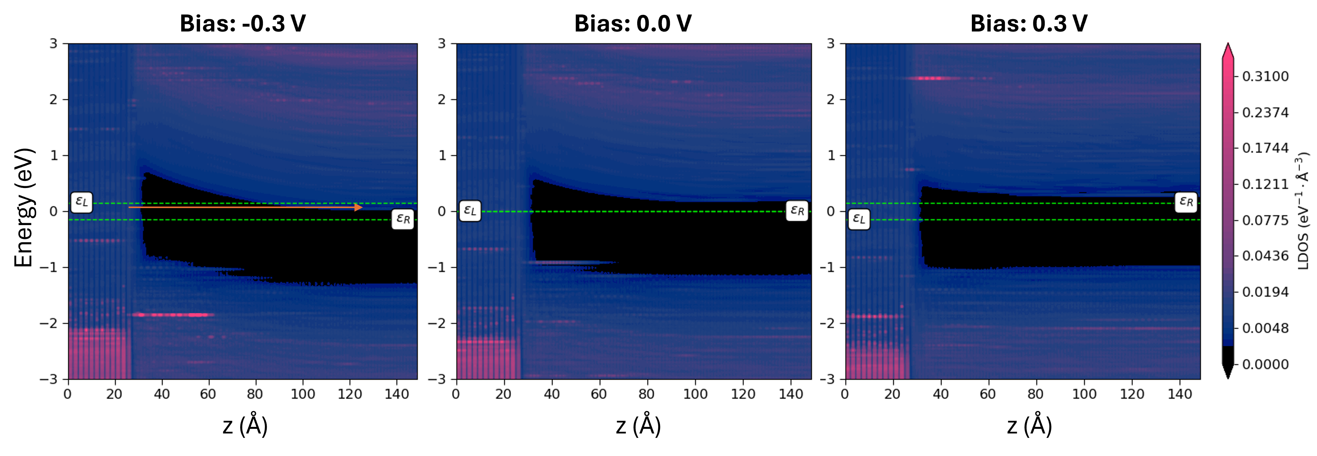
Under negative bias, the band gap appears to bend more noticeably. As the Fermi level of the left (Ag) electrode shifts upward, electrons gain sufficient energy to tunnel through the band gap into the empty states on the Si side. This tunneling leads to a leakage current, which explains the presence of reverse current in the IV characteristics.
Ideality factor
Despite the leakage current at reverse bias, we can investigate the ideality factor of the forward bias. Thermionic emission theory describes the I–V characteristics of a Schottky diode as [8]
where \(q\) is the elementary charge, \(k_B\) is the Boltzmann constant,
\(T\) is the temperature, \(I_0\) is the saturation current, and \(n\)
is the so-called ideality factor. The ideality factor is a measure of how much the
interface resembles an ideal Schottky diode, where a value of \(n\)=1
represents the ideal case. Using a log-plot of \(I/(1-\mathrm{e}^{-qV_{bias}/k_BT})\)
against \(V_{bias}\) you can extract the value of the ideality factor from the
slope. Use the script IV-n-log.py to create such a plot and calculate the ideality
factor. You should edit a few input parameters;
filename: The same .hdf5 file as for IV.py
T: The temperature at which the calculations have been run
numpoints: The number of bias points to include in the fit used to find the ideality factor
Running the script, you should get a value around \(n\)=1.9635, which means that the system deviates significantly from the ideal Schottky diode behavior. As the current in an ideal Schottky diode is dominated by thermonic emission, our steep slope yilding an above one ideality factor suggests additional transport mechanisms are influencing the current flow.
Schottky barrier
The Activation Energy (AE) method [8] is a widely used experimental procedure for extracting the Schottky barrier. The method extracts the Schottky barrier from an Arrhenius-like plot of \(\ln(I/T^2)\) vs. \(1/T\),
Use the script arrhenius.py to calculate the transmission at each applied forward
bias in a range of temperatures between 250 K and 400 K. The transmission is
calculated in a linear-response fashion using the Landauer–Büttiker expression
for the current,
where the transmission coefficient \(T(E,\mu_L,\mu_R)\) has been evaluated self-consistently at a temperature of 300 K during the the IVCurve calculation.
The script needs some inputs to run;
fname1: The .hdf5 file containing the IVCharacteristics analysis
Tmax: Maximum temperature used in the calculations (in K).
Tmin: Minimum temperature used in the calculations (in K).
IF: The calculated ideality factor from IV-n-log.py
voltages: Forward biases for which the calculations have been performed (in V)
fname: Name of output file containing the effective barrier height (in eV)
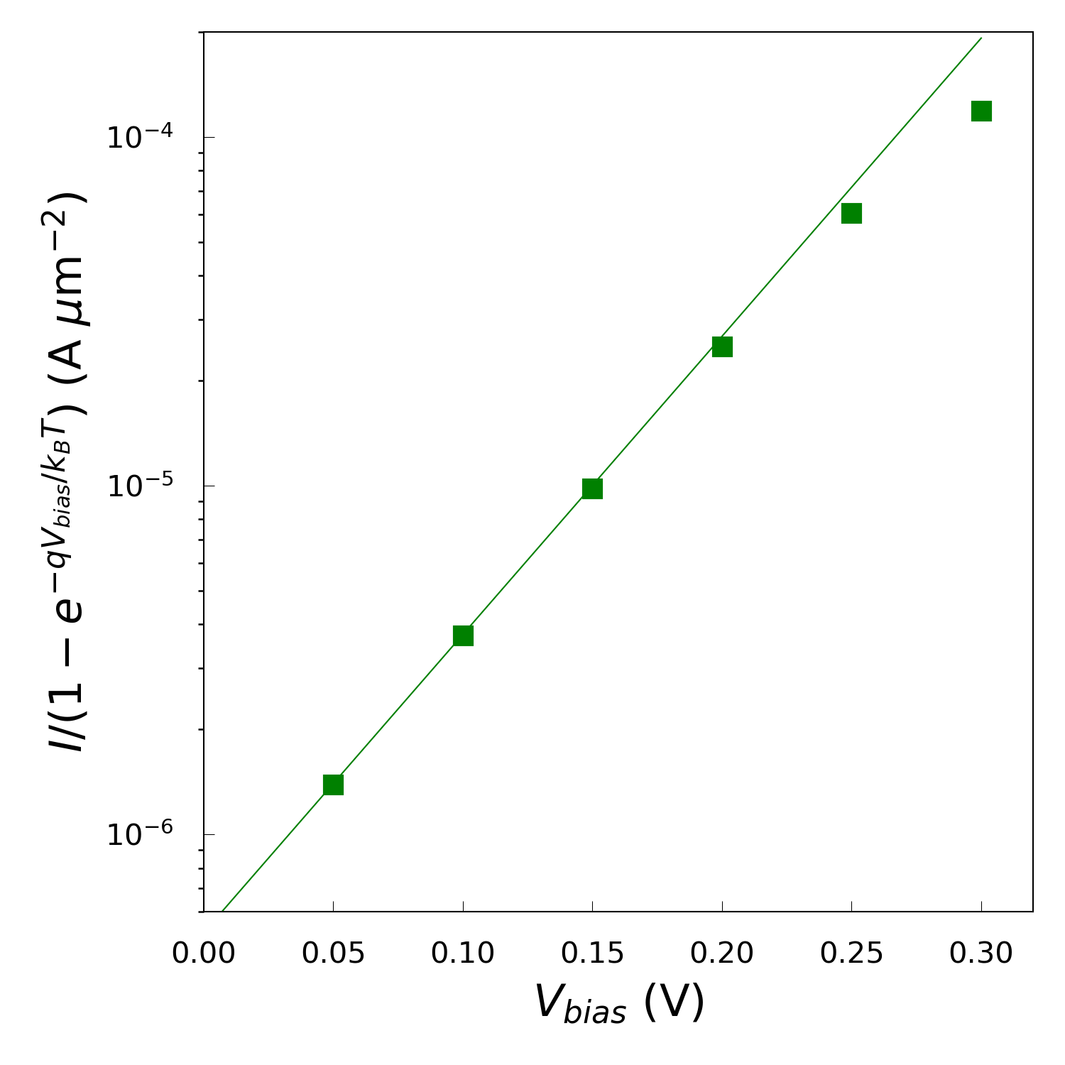
Running the script produces a .dat file containing the I–T characteristics for each of the forward bias points. From these files, the Arrhenius plot seen below is produced:

The linear trend on the logaritmic scale shows an exponential dependence of the current on temperature, consistent with thermally activatec transport. We also observe that as the bias increases, the lines shift upward, meaning the current increases with bias at all temperatures. In the .log file of the script, the Schottky barrier height \(\Phi^{AE}\), from the conduction band minimum of the bulk silicon electrode to the maximum of \(\langle V_H\rangle\), along with the effective barrier height \(\phi^{AE}(V_{bias})\) for each applied bias, are printed:
Bias = 0.05 V
Schottky barrier = 151.86858278688362 meV
Effective barrier = 126.40385143979933 meV

Bias = 0.1 V
Schottky barrier = 173.6608412847027 meV
Effective barrier = 122.73137859053412 meV

Bias = 0.15 V
Schottky barrier = 190.16555474225737 meV
Effective barrier = 113.77136070100454 meV

Bias = 0.2 V
Schottky barrier = 205.25866759729573 meV
Effective barrier = 103.39974220895854 meV

Bias = 0.25 V
Schottky barrier = 219.3404122754261 meV
Effective barrier = 92.01675554000464 meV

Bias = 0.3 V
Schottky barrier = 243.77589450779124 meV
Effective barrier = 90.98750642528553 meV
Notably, the Schottky barrier increases with bias voltage, which is unphysical and should not occur. This suggests that the activation energy (AE) method provides only a limited description of this interface. This limitation is consistent with the extracted ideality factor of 1.96, which indicates that thermionic emission does not dominate the transport. Since the AE method assumes thermionic emission as the primary mechanism, its application here may lead to inaccurate or misleading barrier values.
Analyzing the Spectral current
The final analysis is an investigation of the spectral current which is the energy-resolved distribution of electron flow through a device under bias, showing how different energy states contribute to the total current. This analysis is important because it reveals which regions of the electronic structure dominate transport, highlights resonant states or tunneling features, and helps explain the microscopic mechanisms behind the observed I–V characteristics.
The spectral current is defined as,
We will plot the spectral current and the averaged Hartree difference potential (which we added in the IVCharateristics calculation) together in order to compare the energy of maximum spectral current with the barrier of the Hartree potential.
You can then use hdp_avr.py to calculate the average of each of the potentials. This script is a variation of the hdp.py from earlier and needs the same input parameters, with the difference that this script loads the HartreeDifferencePotential which was run with the IVCharacteristics.
Then, use the script spectral_current.py to plot the averaged potential together with
the spectral current. You need to edit a few parameters:
fname :The .hdf5 file containing the IVCharacteristics analysis
hdp_files: The .dat files containing the averaged potentials
phipot: Schottky barrier calculated with pldos_hdp.py at zero bias (in eV)
CB_min: Conduction band minimum of the bulk Si electrode with respect to the chemical potential of the left electrode, calculated above with pldos_hdp.py (in eV)
fname2: Name of the output file containing the barriers associated with the thermionic emission process (in eV)
fname3: Name of the output file containing the energy of maximum spectral current (in eV)
Running the script should produce the figure below.
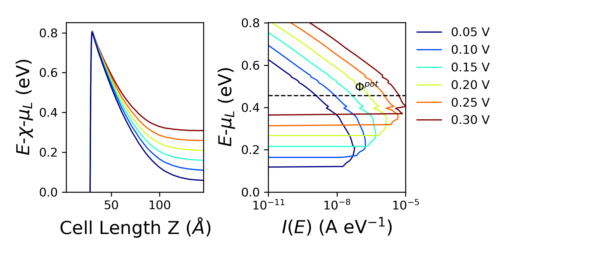
The energy axis of the two plots is aligned by plotting the averaged potential relative to the electron affinity of bulk Si (estimated by pldos_hdp.py) and \(\mu_L\) and the spectral current relative to \(\mu_L\). The left panel shows the potential profile for different bias voltages, where the barrier height increases with the bias, indicating stronger band bending. The right panel displays the spectral current as a function of energy, revealing that higher bias shifts the dominant transport window upward, allowing more states to contribute to conduction. The dashed line marks the potential barrier, highlighting how transport becomes increasingly dominated by energies above this threshold at larger biases.
The script also returns the estimated barrier for thermionic emission, \(\phi_F\), and the energy of maximum spectral current \(Emax\) for each bias both as separate .dat files and printed in the log together.
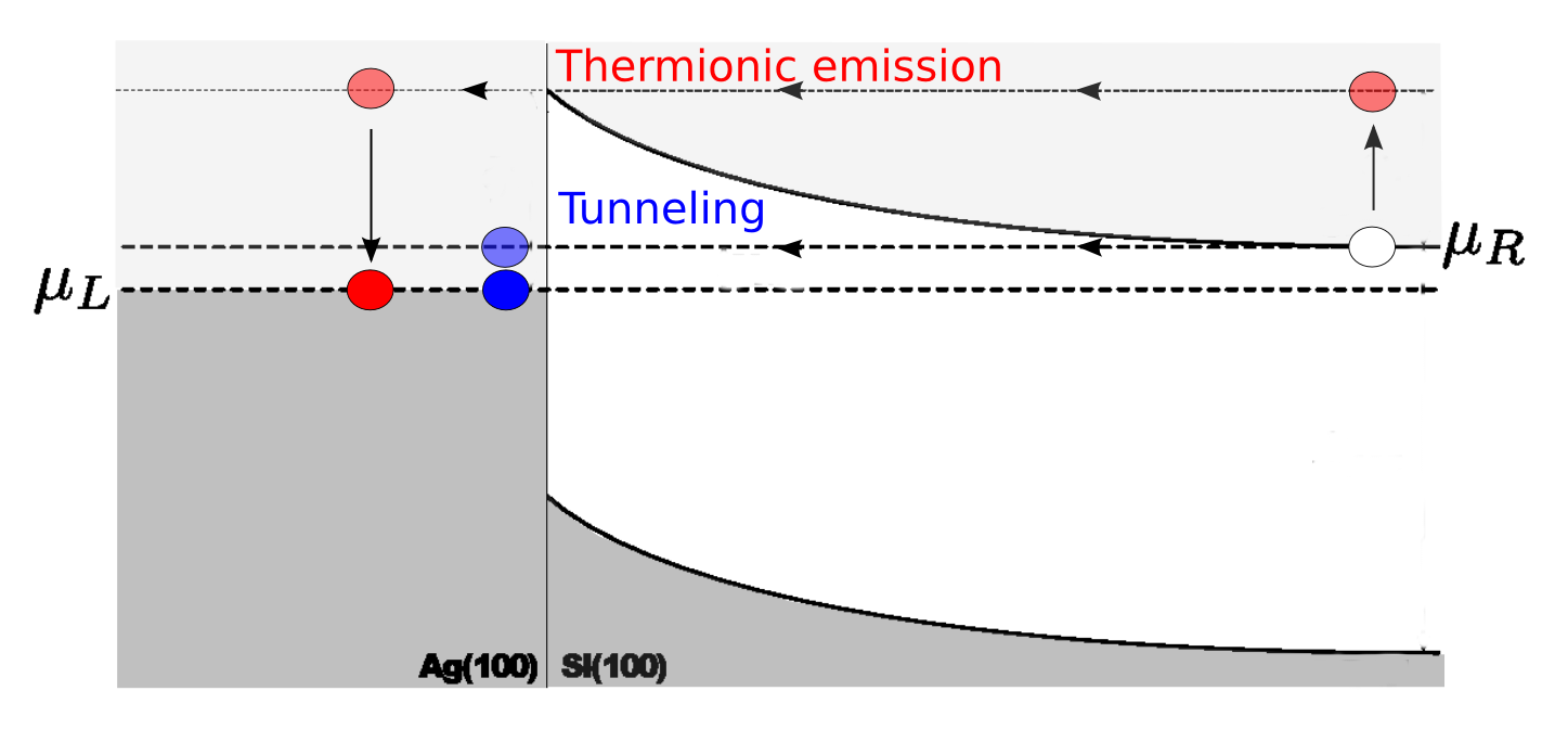
Transmission through the device can occur through two different processes; either by thermionic emission or by tunneling through the Schottky barrier. If the transmission occurs solely by thermionic emission, the spectral current would be zero below \(\Phi^{pot}\). This is definitely not the case. In fact, the energy of maximum spectral current is below the thermionic emission barrier for each bias, revealing that the dominant transmission process is tunneling!
Summing up the results
We compare the finite-bias results by plotting the following:
The energy of maximum spectral current from
spectral_current.py(circles).The thermionic emission barrier \(\phi_F\) from
spectral_current.py(triangles).The effective AE Schottky barrier \(\phi^{AE}(V_{bias})\) from
arrhenius.py(squares).The bias dependence of the AE Schottky barrier predicted by \(\phi^{AE}(V_{bias})\) by using \(\Phi^{AE}=\Phi^{pot}\) (dashed line).
Create the plot using barrier_compare.py. It requires the .dat files created by arrhenius.py
and spectral_current.py along with the calculated ideality factor from IV-n-log.py and the
estimated Schottky barrier at zero bias, \(\Phi^{pot}\), from pldos_hdp.py.
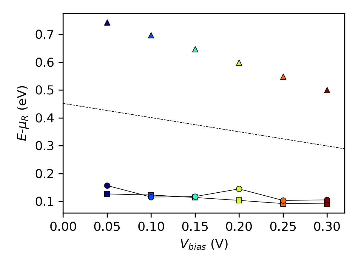
The plot shows that the estimated AE Schottky barrier (squares) lies below the thermionic emission barrier (triangles) for each bias point. This is because the AE method neglects contributions from tunneling and thereby implicitly assumes that the maximum spectral current (circles) will occur at the energy of the barrier height. Furthermore, we see that the analytical bias dependence of the thermionic emission barrier (dashed line) is not in good agreement with the calculated barrier heights (triangles), but the thermionic emission barrier is much higher.
While the activation energy method remains a standard experimental approach for estimating Schottky barrier heights, its application in computational studies, particularly for non-ideal interfaces, can be problematic. The method assumes thermionic emission dominates the current, which is contradicted by the high ideality factor observed in this system. Moreover, the unphysical bias dependence of the extracted barrier height further underscores its limitations.
In contrast, the PLDOS combined with the Hartree difference potential offers a more direct and physically grounded way to visualize and quantify the barrier, especially in systems where tunneling, recombination, or barrier inhomogeneities play a significant role. This suggests that while the AE method is valuable for experimental benchmarking, computational approaches benefit from more nuanced tools that can capture the full complexity of quantum transport. Overall, this section illustrates the importance of critically evaluating traditional methods in light of modern simulation capabilities. It also highlights the need for consistency between modeling assumptions and the physical mechanisms present in the system under study.
Summary
In this tutorial, we demonstrated how to construct and optimize a device, apply the TB09 functional, and approximate the c-parameter for a silicon electrode to improve band gap accuracy. We also showed how to verify whether the depletion layer in a doped system is sufficient.
Next, we explored the limitations of traditional methods for estimating Schottky barrier heights, particularly the activation energy method. We demonstrated that the maximum spectral current occurs below the thermionic emission barrier, indicating that tunneling is the dominant transport mechanism. By comparing different approaches, we highlighted the advantages of using PLDOS and Hartree difference potentials for a more accurate representation of the barrier in non-ideal interfaces.
References
Appendix - Note on the variation of the current
The calculated current is two orders of magnitude lower than the current reported in the publication [1]. This is due to the use of two slightly different Ag electrodes: The silver electrode used in the article was not relaxed after matching the two surfaces at the interface – that electrode is therefore compressed as compared to the Ag electrode used in this case study. This has an impact on the electronic structure of the electrode, which can be shown by comparing the electrode bandstructures:
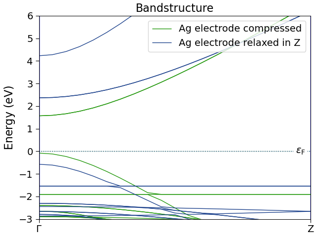
In the figure above, “Ag electrode compressed” is the electrode used in the article, while “Ag electrode relaxed in Z” denotes the electrode used here. Comparing the two, we see that the elongation of the electrode generally results in lower energy levels. The electrode used in this case study has fewer k-points (and thereby states) available in the bias window, which results in smaller transmission and thereby a lower current.