Optical Properties of Silicon
Introduction
The purpose of this tutorial is to show how ATK can be used to compute accurate electronic structure, optical, and dielectric properties of semiconductors from DFT combined with the meta-GGA functional by Tran and Blaha [1] (TB09). TB09 is a semi-empirical functional that is fitted to give a good description of the band gaps in non-metals. The results obtained with the method are often comparable with very advanced many-body calculations, however with a computational expense comparable with LDA, i.e. several order of magnitudes faster. Thus, the TB09 meta-GGA functional is a very practical tool for obtaining a good description of the electronic structure of insulators and semiconductors.
It is important to note that the TB09 functional does not provide accurate total energies [1], and it can therefore only be used for calculating the electronic structure of the materials, while the GGA-PBE functional should be used for computing total energies and atomic geometries.
It is assumed that you are familiar with the general workflow of QuantumATK, as described in the Basic QuantumATK Tutorial.
This tutorial uses silicon as an example. As for most semiconductors, GGA/LDA both severely underestimate the Si band gap (between 0.5 and 0.6 eV), while the experimental band gap of 1.18 eV is reproduced almost exactly by TB09. The experimental dielectric constant is also reproduced by the optical properties module in ATK to within a few percent.
Electronic structure and optical properties of silicon
Setting up the calculation
Start QuantumATK, create a new project and give it a name, then select it and click Open. Launch the Builder by pressing the  icon on the toolbar.
In the builder, click . Type “silicon” in the search field, and select the silicon standard phase in the list of matches. Information about the lattice, including its symmetries (e.g. that the selected crystal is face centered cubic), can be seen in the lower panel.

Double-click the line to add the structure to the Stash, or click the  icon in the lower right-hand corner.
Now send the structure to the Script Generator by clicking the “Send To” icon  in the lower right-hand corner of the window, and select Script Generator (the default choice, highlighted in bold) from the pop-up menu.
In the Script Generator,
Add .
Add .
Add .
Add .
Change the output filename to
si.nc.

The next step is to adjust the parameters of each block, by double-clicking them:
Open the New Calculator
 block, and
select the ATK-DFT calculator (selected by default),
set the k-points to (4,4,4),
select the exchange-correlation functional to MGGA,
under “Basis set/exchange correlation”, set Pseudopotential to HGH[Z=4] LDA.PZ,
and finally select the Tier 3 basis set for Si.
Close the dialogue by clicking OK in the lower right-hand corner
Open the DensityOfStates block, and
select 15 x 15 x 15 kpoints.
Open the OpticalSpectrum block, and
select 15 x 15 x 15 k-points,
use 10 bands below and 20 above the Fermi level (this controls how many bands are included in the calculation of the optical matrix elements).
Note
For this calculation you will use the Hartwigsen, Goedecker, Hutter (HGH) pseudopotentials [2]. The calculation of optical properties requires a good description of virtual states far above the Fermi level. The “Tier 3” basis set for Si consists of optimized 3s, 3p (2 orbitals), 3d, 4s orbitals. Going higher to “Tier 4” would add another 3s orbital, and so on, but this appears to have no significant influence on the band gap (just taking longer time). With a smaller basis set, however, the band gap comes out incorrectly even with TB09-MGGA.
Save the script from the Editor for future reference.
Running and analyzing the calculation
Transfer the script to the Job Manager and start the calculation. The job will finish after a few minutes. The file si.nc should now be visible under Project Files in the main QuantumATK window. On the LabFloor select Group by Item Type.
DOS of silicon
Select the DensityOfStates (gID002), then click the 2D Plot… button on the plugin panel. From the density of states it is possible to determine the band gap of silicon.
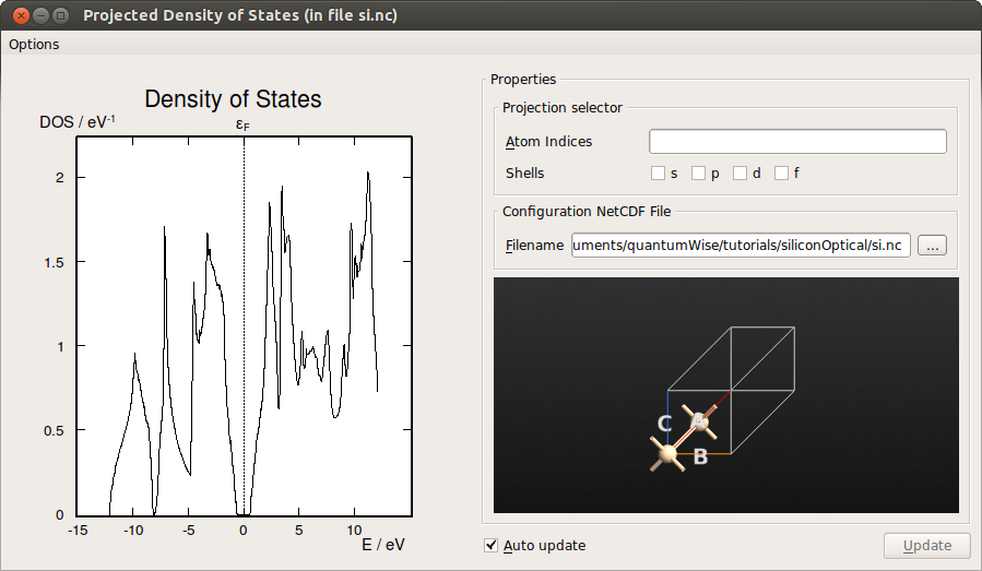
Fig. 35 Density of states (DOS) of Si, computed with meta-GGA.
To read off the band gap, you may zoom the plot or export the DOS data to a file (or simply select Text Representation… instead of 2D Plot…). The band edges are located around -0.59 eV and 0.57 eV, resulting in a band gap of 1.16 eV. This is in excellent agreement with the experimental band gap of 1.17 eV (at 0 Kelvin), in contrast to the LDA band gap of 0.55 eV.
Optical spectrum
Next select the OpticalSpectrum (gID003), then click the 2D Plot… button on the plugin pane. The plot is shown below.
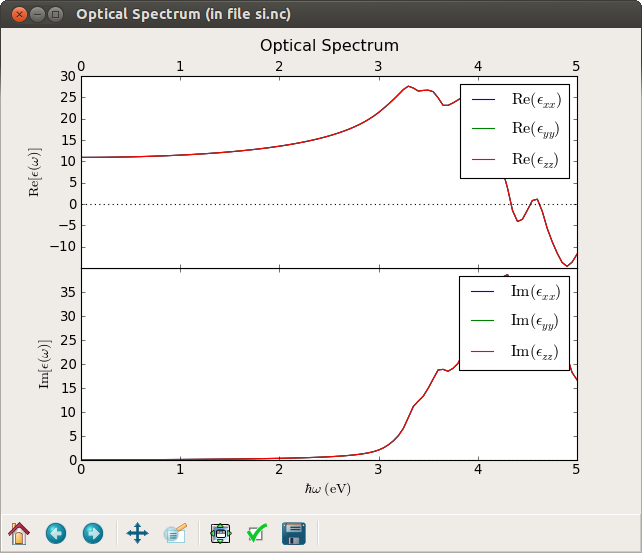
Fig. 36 Real and imaginary parts of the diagonal components of the dielectric constant. Since silicon has cubic symmetry the dielectric constant is isotropic, i.e. \(\epsilon_{xx}=\epsilon_{yy}=\epsilon_{zz}\).
By zooming in (right-click on the plot), in the figure, you can determine the static dielectric constant, \(\mathrm{Re}[\epsilon(\omega=0)]=10.9\), in qualitative agreement with the experimental value of 11.9 (with a bit larger basis set we can get values around 12.2, but also note that we did not optimize the k-point sampling).
The absorption coefficient and refractive index are related to the dielectric constant, see for instance the ATK Reference Manual.
The script below calculates the absorption coefficient and refractive index from the dielectric constant and plots it as a function of the wavelength.
# Load the optical spectrum
spectrum = nlread('si.nc', OpticalSpectrum)[-1]

# Get the energies range
energies = spectrum.energies()

# get the real and imaginary part of the e_xx component of the dielectric tensor
d_r = spectrum.evaluateDielectricConstant()[0, 0, :]
d_i = spectrum.evaluateImaginaryDielectricConstant()[0, 0, :]

# Calculate the wavelength
l = (speed_of_light*planck_constant/energies).inUnitsOf(nanoMeter)

# Calculate real and complex part of the refractive index
n = numpy.sqrt(0.5*(numpy.sqrt(d_r**2+d_i**2)+d_r))
k = numpy.sqrt(0.5*(numpy.sqrt(d_r**2+d_i**2)-d_r))

# Calculate the adsorption coefficient
alpha = (2*energies/hbar/speed_of_light*k).inUnitsOf(nanoMeter**-1)

# Plot the data
import pylab
pylab.figure()
pylab.subplots_adjust(hspace=0.0)
ax = pylab.subplot(211)
ax.plot(l, n, 'b', label='refractive index')
ax.axis([180, 1000, 2.2, 6.4])
ax.set_ylabel(r"$n$", size=16)
ax.tick_params(axis='x', labelbottom=False, labeltop=True)
ax = pylab.subplot(212)
ax.plot(l, alpha, 'r')
ax.axis([180, 1000, 0, 0.24])
ax.set_xlabel(r"$\lambda$ (nm)",  size=16)
ax.set_ylabel(r"$\alpha$ (1/nm)", size=16)
pylab.show()
Save the script to the project folder and execute the script by dropping it on the Job Manager  icon on the toolbar.
The script will generate the figure below.
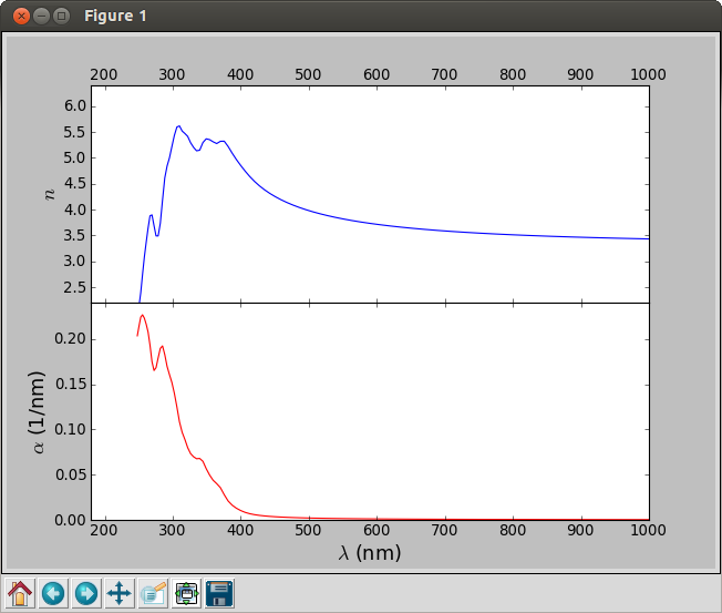
Fig. 37 Refractive index (blue) and adsorption coefficient (red) of silicon as function of the wavelength of the incoming light.