Silicon nanowire field-effect transistor
Version: 2016.0
Introduction
This tutorial shows you how to set up and perform calculations for a device based on a silicon nanowire. You will define the structure of a hydrogen passivated Si(100) nanowire, and set up a field-effect transistor (FET) structure with a cylindrical wrap-around gate. The tutorial ends with calculations of the device conductance as a function of gate bias.
Note
You will primarily use the graphical user interface QuantumATK for setting up and analyzing the results. The underlying calculation engines for this tutorial are ATK-DFT and ATK-SE. A complete description of all the parameters, and in many cases a longer discussion about their physical relevance, can be found in the ATK Reference Manual.

Band structure of a Si(100) nanowire
First step is to set up the Si(100) nanowire and optimize the geometry. You should use the ATK-DFT calculator for this. We then compute the band structure of the nanowire using 3 different computational models; DFT-GGA, DFT-MGGA, and the Extended Hückel method.
Building the nanowire
Open QuantumATK and create a new empty project called “silicon_nanowire”. Then launch the  Builder.
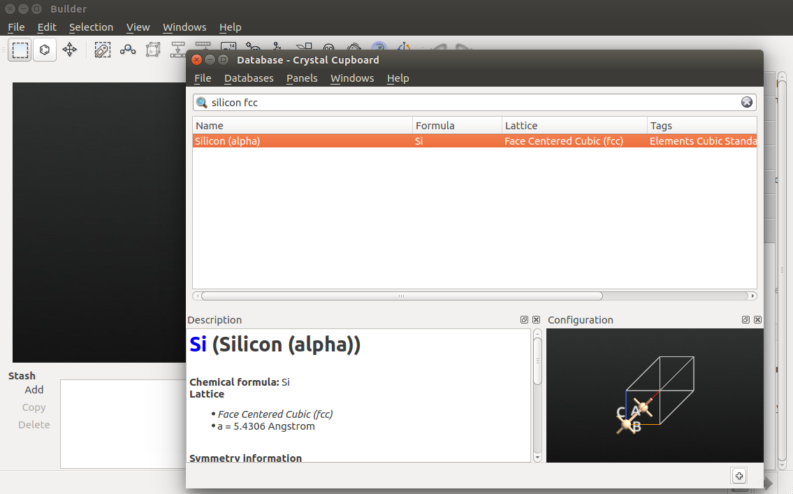
Go to and type “silicon fcc” to locate the diamond phase of silicon.
Add the Silicon (alpha) bulk configuration to the Stash (double-click or use the
 icon).
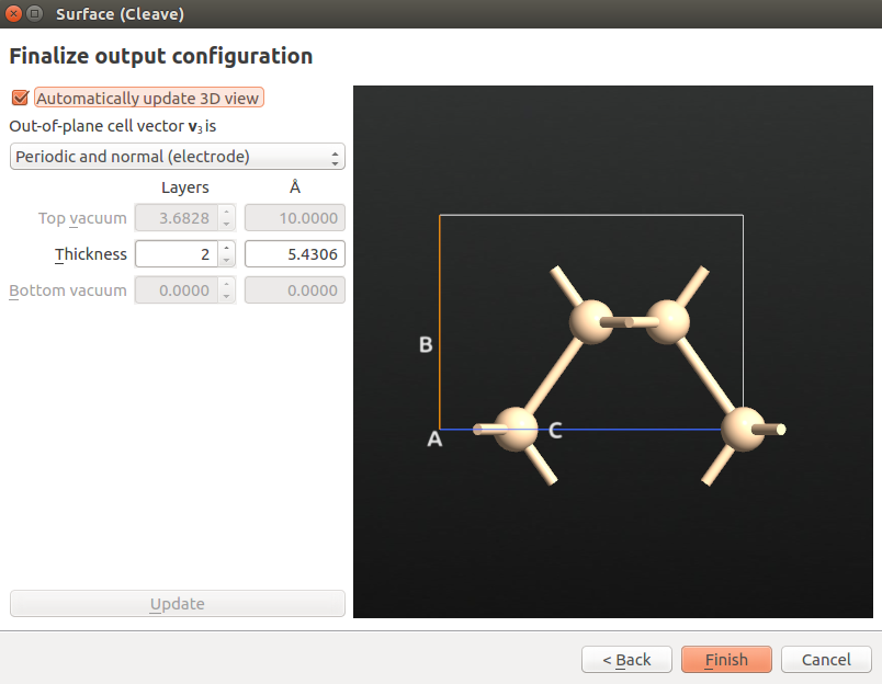
In the Builder, use the tool to create the Si(100) facet:
keep the default (100) cleave direction, and click Next;
keep the default surface lattice, and click Next;
keep the default supercell, which will ensure that the wire direction is perpendicular to the surface, and click Next.
Click Fińish to add the cleaved structure to the Stash.
Next, use the tool to repeat the structure twice along the A and B directions:
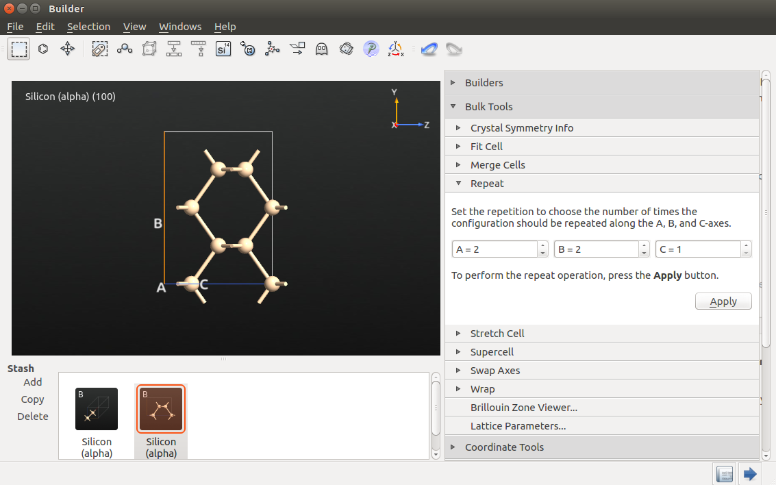
Finalize the nanowire by following these steps:
use the tool to set the A and B lattice vector lengths to 20 Å;
use the tool to center the structure along all directions;
go to and apply the 4(SP3) type hydrogen passivation to the nanowire.

Send the H-passivated Si(100) nanowire to the  Script Generator
by using the
Script Generator
by using the  in the lower right-hand corner of the Builder window.
Setting up and running the calculations
You should now relax the nanowire and compute the band structure. The DFT-GGA method is used for geometry optimization, while the band structure is computed using DFT-GGA, DFT-MGGA, and the Extended Hückel model.
Important
The TB09 meta-GGA and Extended Hückel models can not be used for relaxation.
In the Script Generator, change the default output file
name to si_100_nanowire.hdf5, and add the following blocks to the script:
 New Calculator
 OptimizeGeometry
 Bandstructure
- New Calculator
- Bandstructure
- New Calculator
- Bandstructure
Open the first New Calculator block, and make the following changes
to the calculator settings:
set the k-point sampling to 1x1x11;
change the exchange-correlation potential to GGA.
Open the second New Calculator block, and make the following changes:
set the k-point sampling to 1x1x11;
change the exchange-correlation potential to MGGA.
Open the third New Calculator block, and make the following changes:
select the ATK-SE: Extended Hückel calculator;
uncheck “No SCF iteration” to make the calculation selfconsistent;
set the k-point sampling to 1x1x11;
increase the density mesh cut-off to 20 Hartree;
go to the Hückel basis set tab, and select the “Hoffmann.Hydrogen” and “Cerda.Silicon [GW diamond]” basis sets. The latter has been fitted to GW calculations, and gives an excellent description of the silicon bandstructure, including the value of the band gap.
Finally, open each Bandstructure script block and set the number
of points per segment to 100.
Tip
The default value for the density mesh cut-off is often sufficient, but by increasing it you may sometimes obtain a slightly higher accuracy at a small additional computational cost.
TB09 meta-GGA c-parameter
You should also adjust the value of the c-parameter used in the TB09 meta-GGA method. This is essentially a fitting parameter that can be used to adjust the calculated band gap of the material. If the c-parameter is not defined by the user, a value is automatically calculated from the electronic structure of the material. However, this will not work for a system with vacuum regions, like a nanowire.
You will therefore use a fixed value, c=1.0364, which has been fitted to yield an accurate prediction of the fundamental band gap in silicon (1.13 eV).
Transfer the QuantumATK Python script to the  Editor using the icon.
Then locate the script line defining the variable
Editor using the icon.
Then locate the script line defining the variable exchange_correlation for the MGGA
exchange-correlation, and set the fixed value of c to 1.0364, as illustrated below.
#----------------------------------------
# Exchange-Correlation
#----------------------------------------
exchange_correlation = MGGA.TB09LDA(c=1.0364)
Running the calculations
Save the QuantumATK Python script as si_100_nanowire.py and execute it using the
 Job Manager. It will take just a few minutes to complete the calculations.
Analyzing the results
Once the calculations have finished, the HDF5 data file si_100_nanowire.hdf5
should appear on the QuantumATK LabFloor. Locate the Bandstructure items inside this file.
The order of the item IDs corresponds to the order in which the band structures were
computed and saved, i.e. GGA, MGGA, and Hückel.
Select one of the band structures and open the Bandstructure Analyzer in the right-hand Panel Bar to inspect the computed band structure. You can do this for all three band structures, or use the Compare Data plugin to plot a direct comparison of the three band structures.
Detailed band structure analysis
In order to compare the band gaps obtained with the three computational models,
it is convenient to use bandstructure_analyzer.py, which uses QuantumATK Python for detailed analysis
of the gaps in a band structure. The script is shown below:
  1from QuantumATK import *
  2import pylab
  3# Custom analyzer for calculating the band gap of a bandstructure
  4
  5#helper function to find minima
  6def fitEnergyMinimum (i_min, energies, k_points, nfit=3):
  7    """
  8    Function for fitting the energy minimum located around i_min.
  9
 10    @param i_min   : approximate position of the energy minimum.
 11    @param energies: list of energies.
 12    @param k_points: list of k_points which correspond to the energies.
 13    @param nfit    : order of the polynomium.
 14    @return d2_e, e_min, k_min : second derivative of energy,
 15                                 minimum energy, minimum k_point.
 16    """
 17    #list of energies
 18    n = len(energies)
 19    efit = numpy.array([energies[(n+i_min-nfit/2+i)%n] for i in range(nfit)])
 20    kfit = numpy.array([i-nfit/2 for i in range(nfit)])
 21    #special cases
 22    if i_min == 0: #assume bandstructure symmetric around zero
 23        for i in range(nfit/2):
 24            efit[i] = energies[nfit/2-i]
 25
 26    if i_min == n-1: #assume bandstructure symmetric around end point
 27        for i in range(nfit/2+1, nfit):
 28            efit[i] = energies[n-1+nfit/2-i]
 29
 30    #make fit
 31    p = numpy.polyfit(kfit,efit,2)
 32    i_fit_min = -p[1]/2./p[0]
 33    pf = numpy.poly1d(p)
 34    e_min = pf(i_fit_min)
 35    i0 = int(i_fit_min+i_min+n)
 36    w = i_fit_min+i_min+n-i0
 37    k_min = (1-w)*k_points[i0%n]+w*k_points[(i0+1)%n]
 38
 39    return p[0], e_min, k_min
 40
 41def analyseBandstructure(bandstructure, spin):
 42    """
 43    Function for analysing a band structure and calculating bandgaps.
 44
 45    @param bandstructure :  The bandstructure to analyze
 46    @param spin          :  Which spin to select from the bandstructure.
 47    @return  e_val, e_con, e_gap :  maximum valence band energy,
 48                                    minimum conduction band energy,
 49                                    and direct band gap.
 50    """
 51    energies = bandstructure.evaluate(spin=spin).inUnitsOf(eV)
 52
 53    #some placeholder variable to help finding the extrema
 54    e_valence_max = -1.e10
 55    e_conduction_min = 1.e10
 56    e_gap_min = 1.e10
 57    i_valence_max = 0
 58    i_conduction_min = 0
 59    i_gap_min = 0
 60    n_valence_max = 0
 61    n_conduction_min = 0
 62    n_gap_min = 0
 63
 64    # Locate extrema
 65    for i in range(energies.shape[0]):
 66        # find first state below Fermi level
 67        n = 0
 68        while n < energies.shape[1] and energies[i][n] < 0.0:
 69            n += 1
 70
 71        # find maximum of valence band
 72        if (energies[i][n-1] > e_valence_max):
 73            e_valence_max = energies[i][n-1]
 74            i_valence_max = i
 75            n_valence_max = n-1
 76        # find minimum of conduction band
 77        if (energies[i][n] < e_conduction_min):
 78            e_conduction_min=energies[i][n]
 79            i_conduction_min=i
 80            n_conduction_min=n
 81        # find minimum band gap
 82        if (energies[i][n]-energies[i][n-1] < e_gap_min):
 83            e_gap_min = energies[i][n]-energies[i][n-1]
 84            i_gap_min = i
 85            n_gap_min = n-1
 86
 87    # Print out results
 88    a_val, e_val, k_val = fitEnergyMinimum(i_valence_max,
 89                                           energies[:,n_valence_max],
 90                                           bandstructure.kpoints())
 91    print('Valence band maximum    %7.4f eV at [%6.4f, %6.4f,%6.4f]   ' \
 92                         %(e_val, k_val[0], k_val[1], k_val[2]))
 93
 94    a_con, e_con, k_con = fitEnergyMinimum(i_conduction_min,
 95                                           energies[:,n_conduction_min],
 96                                           bandstructure.kpoints())
 97    print('Conduction band minimum %7.4f eV at [%6.4f, %6.4f,%6.4f]   ' \
 98                         %(e_con, k_con[0], k_con[1], k_con[2]))
 99
100    print('Fundamental band gap    %7.4f eV ' % (e_con-e_val))
101
102    a_gap, e_gap, k_gap = fitEnergyMinimum(i_gap_min,
103                           energies[:,n_gap_min+1]- energies[:,n_gap_min],
104                           bandstructure.kpoints())
105
106    print('Direct band gap         %7.4f eV at [%6.4f, %6.4f,%6.4f]   ' \
107                        %(e_gap, k_gap[0], k_gap[1], k_gap[2]))
108    return e_val, e_con, e_gap
109
110def analyzer(filename, **args):
111    """
112    Find band gaps of band structures in netcdf file.
113    """
114
115    if filename == None:
116        return
117
118    #read in the bandstructure you would like to analyze
119    bandstructure_list = nlread(filename, Bandstructure)
120    if len(bandstructure_list) == 0 :
121        print('No Bandstructures in file ', filename)
122        return
123
124    for s in [Spin.All]:
125        b_list = []
126        n = 0
127        for b in bandstructure_list:
128            print('Analyzing bandstructure number ', n)
129            b_list = b_list + [analyseBandstructure(b,s)]
130            print()
131            print()
132            n += 1
133
134        x = numpy.arange(len(b_list))
135        e_val =  numpy.array([b[0] for b in b_list])
136        e_con =  numpy.array([b[1] for b in b_list])
137        e_indirect = e_con-e_val
138        e_direct = numpy.array([b[2] for b in b_list])
139
140
141analyzer("si_100_nanowire.hdf5")
Download the script (link: bandstructure_analyzer.py), and execute it using the Job Manager.
You should get the following output:
Analyzing bandstructure number  0
Valence band maximum    -1.6395 eV at [0.0000, 0.0000,0.0121]
Conduction band minimum  1.6400 eV at [0.0000, 0.0000,0.0000]
Fundamental band gap     3.2795 eV
Direct band gap          3.2799 eV at [0.0000, 0.0000,0.0000]


Analyzing bandstructure number  1
Valence band maximum    -1.8434 eV at [0.0000, 0.0000,0.1501]
Conduction band minimum  1.8450 eV at [0.0000, 0.0000,0.0000]
Fundamental band gap     3.6884 eV
Direct band gap          3.6914 eV at [0.0000, 0.0000,0.0026]


Analyzing bandstructure number  2
Valence band maximum    -1.7737 eV at [0.0000, 0.0000,0.0000]
Conduction band minimum  1.7735 eV at [0.0000, 0.0000,0.0000]
Fundamental band gap     3.5472 eV
Direct band gap          3.5472 eV at [0.0000, 0.0000,0.0000]
The output shown above gives the band structure analysis for the DFT-GGA, DFT-MGGA, and Extended Hückel models. The script gives the valence band maximum, conduction band minimum, fundamental band gap, and direct band gap from the valence band maximum. The fundamental band gap for the Si(100) nanowire is significantly larger than that of bulk silicon, and all three computational models place it at the Gamma point or close to it.
Furthermore, the TB09-MGGA model gives a gap which is about 0.5 eV larger than the GGA model, which is in accordance with the difference in the band gaps of bulk Si calculated with the GGA and TB09-MGGA methods. The Extended Hückel model is in agreement with the TB09-MGGA method.
Si(100) nanowire FET device
You will now consider a Si(100) nanowire field-effect transistor with a cylindrical wrap-around gate. You should first build the device configuration, including the gate and doping of the silicon nanowire, and then use the Extended Hückel model to compute device properties such as zero-bias transmission and conductance vs. gate voltage.
FET device configuration
You should use the relaxed nanowire configuration as a starting point for building
the device. The contents of the file si_100_nanowire.hdf5 should be available
on the QuantumATK LabFloor. It contains four bulk configurations: The first one (gID000)
is the unrelaxed structure, while the remaining ones correspond to the relaxed structure,
calculated with different methods (DFT-GGA, DFT-MGGA and Extended Hückel).
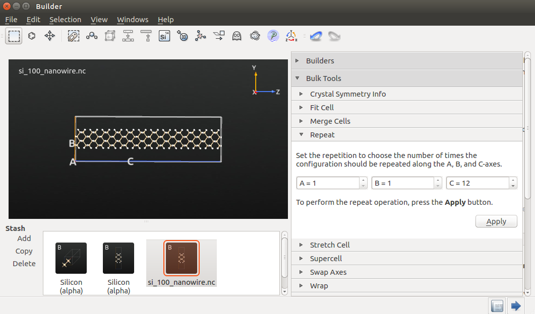
Send the configuration with ID gID001 to the Builder. It will
appear in the Builder Stash. Then use the
tool to repeat the configuration 12 times along C.
Setting up the gate
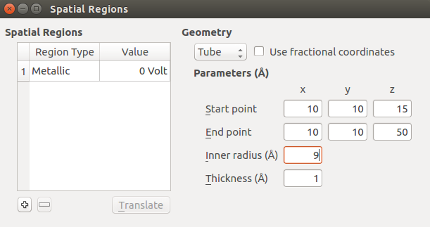
Next, use the tool to define the metallic wrap-around gate:
First, add a new metallic region with a value of 0 Volt.
Under Geometry, select Tube to create a cylindrical region.
Define the geometry of the tube by entering the parameters shown in the image below. The cylinder will extend to the edge of the simulation cell along A and B, and will cover most of the central part of the nanowire along C.
Build the device
Use the tool to build the Si(100) nanowire FET device from the bulk nanowire configuration. Use the default suggestion for the electrode lengths.
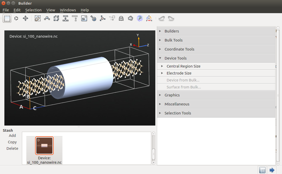
Then send the device configuration to the Script Generator.
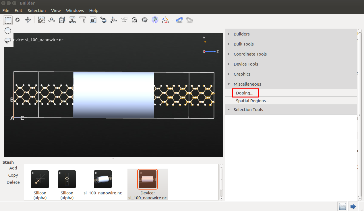
Doping the Si(100) wire
You will now introduce doping in the nanowire. Instead of explicitly adding dopant atoms, which would result in a very high doping concentration for this relatively small device, you will set up the system as a p-i-n junction, by adding certain amounts of charge to the electrodes. This will lead to shifts in the Fermi levels of the two electrodes, resulting in a built-in potential in the device.
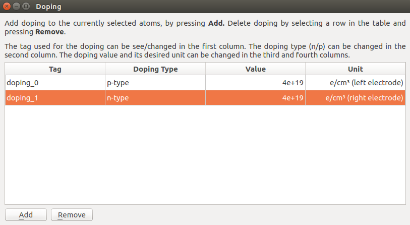
Use the mouse to select all atoms in the left electrode and open the tool. In the window that shows up, choose the following settings:
Doping Type: p-type
Value: 4e+19
Unit: e/cm3 (left electrode)
Next, close the Doping window and select all atoms in the right electrode. Open again the Doping tool, and choose the following settings:
Doping Type: n-type
Value: 4e+19
Unit: e/cm3 (right electrode)
Zero gate voltage calculation
You will now calculate the transmission spectrum of the p-i-n doped Si(100) nanowire
FET device at zero gate potential using the Extended Hückel model. In the
Script Generator, change the default output file name to si_100_nanowire_fet_pin.hdf5
and add the following blocks to the script:
- New Calculator
- TransmissionSpectrum
- ElectronDifferenceDensity
- ElectrostaticDifferencePotential
Open the New Calculator block, select the Extended Hückel
device calculator, and set up the calculator parameters similarly to what you
did above for the bulk nanowire calculations:
Uncheck “No SCF iteration” to make the calculation selfconsistent.
Increase the density mesh cut-off to 20 Hartree.
Go to the Hückel basis set tab and select the “Hoffmann.Hydrogen” and “Cerda.Silicon [GW diamond]” basis sets.
Under Poisson solver, use Neumann boundary conditions in the A and B directions.
In the TransmissionSpectrum block, set the energy range to -4 to +4 eV with 301 points.
Save the QuantumATK Python script as si_100_nanowire_fet_pin.py and execute it
using the Job Manager. The calculation will take about 30 minutes
if executed in parallel with 4 MPI processes.
Note
It would be physically incorrect to use periodic boundary conditions along the A and B directions when there are gates present in the system. We therefore choose Neumann boundary conditions along A and B instead.
Analyzing the results
Once the calculation is completed, locate the file si_100_nanowire_fet_pin.hdf5
HDF5 file on the Labfloor and unfold it. Select the TransmissionSpectrum item
and use the Transmission Analyzer to plot the transmission spectrum.
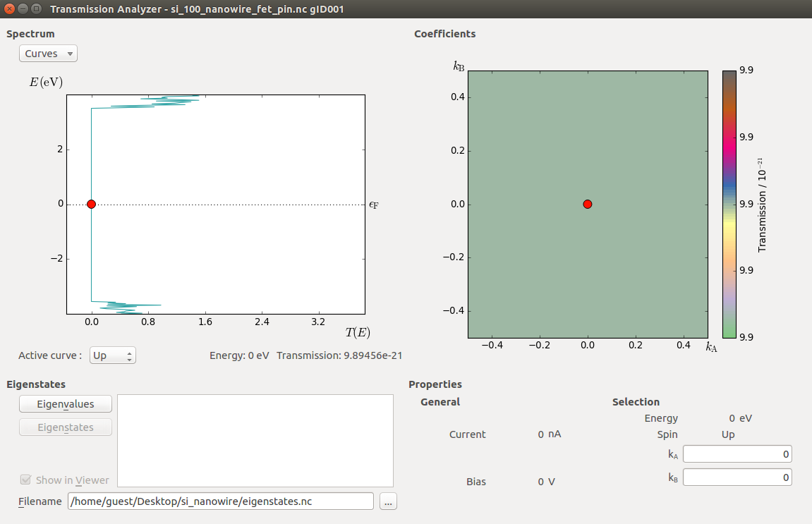
The transmission spectrum is shown above. The transmission is zero inside the nanowire band gap, which appears to be roughly 7 eV, significantly larger than computed earlier. This is due to the p- and n-doping, which has moved the valence and conduction band edges with respect to the Fermi level.
Performing a gate scan
Finally, you will calculate the transmission spectrum for different values of the gate bias. You can then plot the device conductance as function of gate bias.
The calculations are most conveniently done using QuantumATK Python scripting. Use the script
nanodevice_gatescan.py for this. Download it to the active QuantumATK project folder, which also contains
the file si_100_nanowire_fet_pin.hdf5. The script is reproduced below.
 1# Read in the old configuration
 2device_configuration = nlread("si_100_nanowire_fet_pin.nc",DeviceConfiguration)[0]
 3calculator = device_configuration.calculator()
 4metallic_regions = device_configuration.metallicRegions()
 5
 6# Define gate_voltages
 7gate_voltage_list=[-1, 0, 1.0, 2.0, 3.0, 4.0, 5.0, 6, 7, 8,]*Volt
 8# Define output file name
 9filename= "nanodevice_huckel.nc"
10
11# Perform loop over gate voltages
12for gate_voltage in gate_voltage_list:
13    # Set the gate voltages to the new values
14    new_regions = [m(value = gate_voltage) for m in metallic_regions]
15    device_configuration.setMetallicRegions(new_regions)
16
17    # Make a copy of the calculator and attach it to the configuration
18    # Restart from the previous scf state
19    device_configuration.setCalculator(calculator(),
20         initial_state=device_configuration)
21    device_configuration.update()
22    nlsave(filename, device_configuration)
23
24    # Calculate analysis objects
25    electron_density = ElectronDifferenceDensity(device_configuration)
26    nlsave(filename, electron_density)
27
28    electrostatic_potential = ElectrostaticDifferencePotential(device_configuration)
29    nlsave(filename, electrostatic_potential)
30
31    transmission_spectrum = TransmissionSpectrum(
32        configuration=device_configuration,
33        energies=numpy.linspace(-4,4,301)*eV,
34        kpoints=MonkhorstPackGrid(1,1),
35        energy_zero_parameter=AverageFermiLevel,
36        infinitesimal=1e-06*eV,
37        )
38    nlsave(filename, transmission_spectrum)
39    nlprint(transmission_spectrum)
Execute the script using the Job Manager or from a command
line. The script consists of 8 different calculations and it will take about 5 hours
running in parallel with 4 MPI processes. You can, however, decide to reduce this
time by reducing the number of gate voltages that the transmission spectrum is computed
for – simply edit the variable gate_voltage_list.
Analyzing the gate scan
Download and execute the script conductance_plot.py, which reads the computed transmission spectra,
calculates the conductance for each, and plots the conductance against gate bias.
 1# Read the data
 2transmission_spectrum_list = nlread("nanodevice_huckel.hdf5", TransmissionSpectrum)
 3configuration_list = nlread("nanodevice_huckel.hdf5", DeviceConfiguration)
 4
 5conductance = numpy.zeros(len(configuration_list))
 6gate_bias = numpy.zeros(len(configuration_list))
 7for i, configuration in enumerate(configuration_list):
 8    transmission_spectrum = transmission_spectrum_list[i]
 9    energies = transmission_spectrum.energies().inUnitsOf(eV)
10    spectrum = transmission_spectrum.evaluate()
11    gate_bias[i] = configuration.metallicRegions()[0].value().inUnitsOf(Volt)
12    conductance[i] = transmission_spectrum.conductance()
13
14# Sort the data according to the gate bias
15index_list = numpy.argsort(gate_bias)
16
17# Plot the spectra
18import pylab
19pylab.figure()
20ax = pylab.subplot(111)
21ax.semilogy(gate_bias[index_list],  conductance[index_list])
22ax.set_ylabel("Conductance (S)", size=16)
23ax.set_xlabel("Gate Bias (Volt)", size=16)
24ax.set_ybound(lower=1e-26)
25
26for g,c in zip(gate_bias[index_list],  conductance[index_list]):
27    print(g,c)
28pylab.show()
