Atomic-scale capacitance
Version: P-2019.03
In this tutorial you will perform an atomic-scale simulation of a parallel plate nano-capacitor, which means that the gap between the two parallel metal surfaces is in the nanometer range. This is currently not a realistic device, but the purpose is to show a methodology that can be used to compute the capacitance of other structures, including metal/semiconductor/metal structures.

Attention
Capacitor physics Applying a bias \(V\) across the capacitor leads to a build-up of oppositely signed charge \(Q\) on the plates, and therefore an electric field \(E\) between them. The electric field strength can be written as \(E=\sigma/\varepsilon = V/d\), where \(\sigma = Q/A\) is the charge density and \(\varepsilon = k \varepsilon_0\) is the permittivity of the spacer layer between the plates (vacuum or dielectric). The capacitance can then be calculated from \(C = Q/V = Q / Ed = A \varepsilon/d\), where \(d\) is the distance between the plates.
Calculations The equations given above are valid for an ideal macroscopic parallel plate capacitor, but a nano-scale capacitor may in general be quite different. The main method used for computing the capacitance from first principles is to evaluate the electrostatic energy, and from that the capacitance. We will also show a slightly simpler approach based on the Mulliken charge populations of the atoms.

Build the parallel plate capacitor
Open the Builder  , and do the following:
Use to add gold to the Stash.
Open the plugin, and create a Au(111) electrode by entering the Miller indices as [111].
Repeat the structure 8 times in the C direction using .
Select and delete the two atoms in the middle – they have atom indices 19 and 4.
Select the surface atoms (indices 10 and 11 after deletion), and turn them into ghost atoms using the toolbar icon
 .
.Turn the bulk structure into a device configuration via and use the default settings.
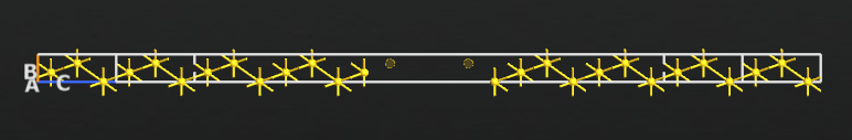
The result will be the device as shown below.
Note
The ghost atoms are used to improve the description of the electron density between the two surfaces. They are simply extra basis sets placed in the empty region. This technique, which is sometimes referred to as a vacuum basis, is also used for calculating the work function of a surface, as explained in a tutorial: Computing the work function of a metal surface using ghost atoms.
Calculations
Zero bias
Send the device configuration to the Script Generator  by clicking the
  icon, and set up the script as follows:
Add an LCAOCalculator
 and use the DFT-LDA engine
with a SingleZetaPolarized basis set. Then set a 5x5x101 k-point grid.
and use the DFT-LDA engine
with a SingleZetaPolarized basis set. Then set a 5x5x101 k-point grid.
Change the output filename to
au_vacuumgap.hdf5.Save the script as
au_vacuumgap.py.
Send the script to the Job Manager  and execute
the calculation. It takes 3-4 minutes on a laptop.
and execute
the calculation. It takes 3-4 minutes on a laptop.
Finite bias
To compute the capacitance it is necessary to compute \(dq/dV\),
where \(dq\) is the induced charge on the surfaces and \(V\)
the bias voltage. In the bias voltage you will also run the following analysis
objects  : MullikenPopulation,
ElectrostaticDifferencePotential, and ElectronDifferenceDensity.
: MullikenPopulation,
ElectrostaticDifferencePotential, and ElectronDifferenceDensity.
Use the following script to perform the calculations for bias voltages of 0.25, 0.5, 0.75, and 1.0 V:
device_configuration = nlread('au_vacuumgap.hdf5', DeviceConfiguration)[-1]
calculator = device_configuration.calculator()
for voltage in [0.0, 0.25, 0.5, 0.75, 1.0]:
    # Set new calculator with modified electrode voltages on the configuration
    # use the self consistent state of  the old calculation as starting input.
    device_configuration.setCalculator(
          calculator(electrode_voltages=(0.5*voltage*Volt, -0.5*voltage*Volt)),
                     initial_state=device_configuration)
    device_configuration.update()
    nlsave('au_vacuumgap.hdf5', device_configuration, object_id="SCF %s" % voltage)
    # -------------------------------------------------------------
    # Mulliken population
    # -------------------------------------------------------------
    mulliken_population = MullikenPopulation(device_configuration)
    nlsave('au_vacuumgap.hdf5', mulliken_population, object_id="Mulliken %s" % voltage)
    # -------------------------------------------------------------
    # Electrostatic difference potential
    # -------------------------------------------------------------
    electrostatic_difference_potential = ElectrostaticDifferencePotential(device_configuration)
    nlsave('au_vacuumgap.hdf5', electrostatic_difference_potential, object_id="EDP %s" % voltage)
    # -------------------------------------------------------------
    # Electron difference density
    # -------------------------------------------------------------
    electron_difference_density = ElectronDifferenceDensity(device_configuration)
    nlsave('au_vacuumgap.hdf5', electron_difference_density, object_id="EDD %s" % voltage)
You can download the scipt here:
bias_loop.py.
Run it using the Job Manager or execute it from a terminal:
$ atkpython bias_loop.py > bias_loop.out
It takes about half an hour to finish this calculation on a laptop.
Note
The previously converged calculation is used as an initial guess for
the next calculation to speed up the SCF convergence. The object_id
makes it easier to identify the data in post-SCF analysis.
Analysis
We will introduce two different ways to calculate the capacitance:
a simple approach based on the induced charge;
a more general method based on evaluating the electrostatic energy.
Approach based on the induced charge
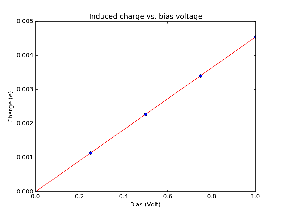
The finite bias will build up a net positive/negative charge on the two gold surfaces, as shown in the plots below.
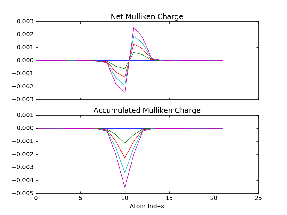
Now, the capacitance can in principle be computed as \(C=dq/dV\), where \(q\) is the total accumulated charge on one surface as a function of the bias. From the slope of the straight line you can therefore obtain the capacitance of the nano-capacitor:
The plots above, as well as the entire data analysis based on the Mulliken
populations, can be achieved by running this script:
mulliken-analysis.py.
It is a long script but a great opportunity to learn about custom data
analysis in Python and QuantumATK.
Results
The script reports a capacitance of 7.27*10-22 Farad, as computed from fitting a straight line to the data points. To put this number into perspective, consider the capacitance of an ideal parallel plate capacitor, written as \(C = \varepsilon A/d\), where \(\varepsilon=1\) for the vacuum permittivity and the area \(A\) of each plate can be calculated from the device structure. You can then calculate the parallel plate distance \(d=A/C\). This is also done in the script and it reports \(d\)=8.77 Å.
Comparing this value with the distance between the surface gold atoms (11.89 Å) the position of the so-called image plane is estimated to be 1.56 Å above the gold surface.
Electrostatic energy analysis
To compute the capacitance using a more general and accurate method, you will need to first calculate the electrostatic energy \(E\) as a function of the applied bias \(V\):
where \(\delta v\) is the induced electrostatic potential and \(\delta n\) is the induced density.
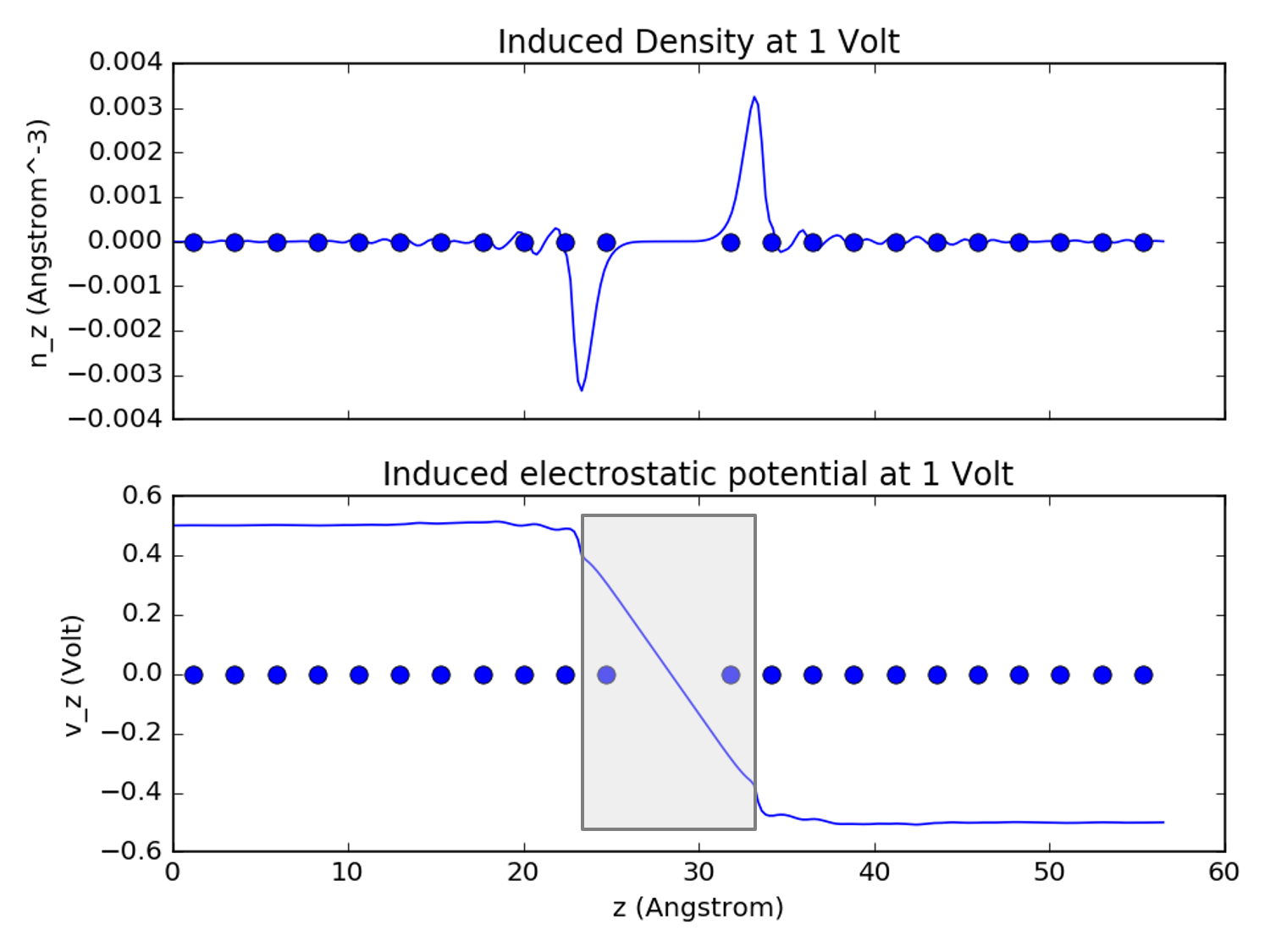
The script potential_plot.py
extracts the potential and density at 1 V bias from the existing HDF5
file and produces the plots of the induced density and electrostatic potential.
The script also reports two parameters:
the electric field in the middle of the vacuum gap \(E\)= 0.1127 V/Å;
the distance between the two image planes \(d\)=8.88 Å.
Tip
The position of the image planes is defined as the point where the electric field is zero, that is, where the electrostatic potential becomes flat.

The blue circles correspond to the atom positions. The main charge accumulation takes place in a very narrow region right above the surface, between the outer surface atoms and the ghost atoms.
From this, the capacitance can be extracted by fitting a parabola to the
relation \(E(V) = CV^2/2\). The script
v-e-plot.py
calculates the electrostatic energy and fits the capacitance as shown below.
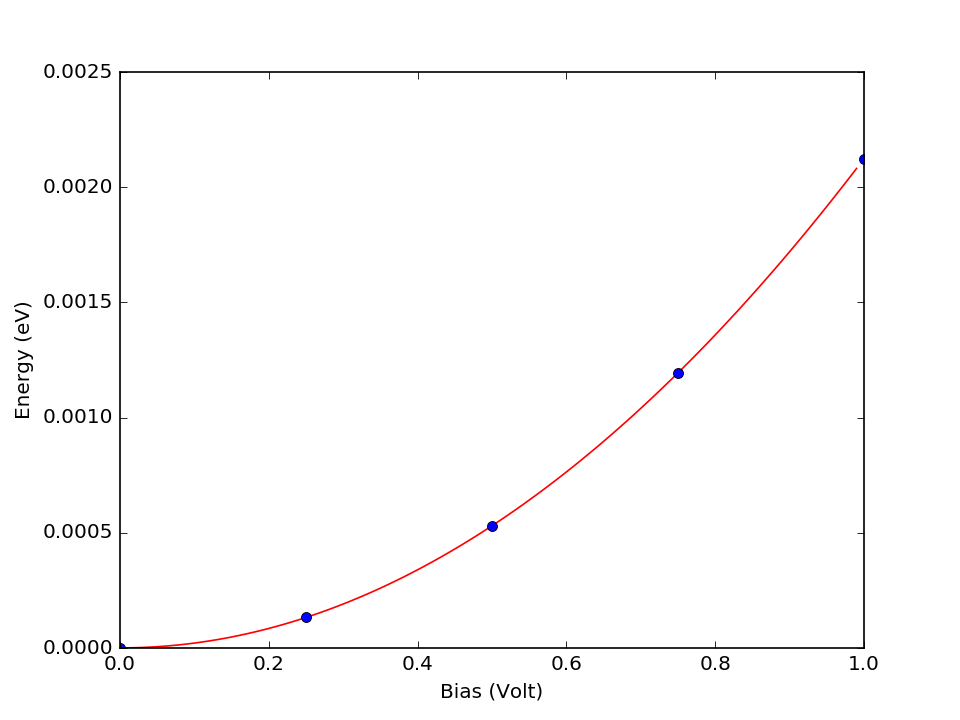
Results
The script reports the capacitance \(C\)=6.81*10-22 Farad, in qualitative agreement with the value obtained from the simple approach using Mulliken charge analysis.
This script also reports \(d\)=9.36 Å, corresponding to an image plane at 1.27 Å above the gold surface, in very close accordance with the position of the peak of induced density.
Attention
What is the difference between the two methods? In the Mulliken charge analysis, it is assumed that all electrons on the left surface have the same potential, and similarly for the right surface. When we convolute the electron density and the electrostatic potential we account for the fact that some part of the electron density is located in the region with a finite electric field. The electrostatic energy analysis is therefore more accurate for calculating the capacitance.
The electrostatic energy analysis also has the advantage that it does not require the researcher to separate the atoms as uniquely “left” and “right” – this is trivial for the two gold surfaces, but that may not always be the case.
Bias-dependent capacitance
The analysis outlined above is based on the assumption that the capacitance is independent of the voltage. However, this is not always the case. A more advanced spline curve fitting allows you to investigate systems whose capacitance does depend on the bias voltage.
Provided that you have already run the scripts mulliken-analysis.py
and v-e-plot.py in the previous section, you can now download and
run the script v-c-plot.py
to perform the fitting.
Note
The data saved by the two scripts are used by the present script to accelerate the analysis.
The computed capacitance is shown below as a function of the bias. As expected, the capacitance changes in this case very little with the bias voltage.
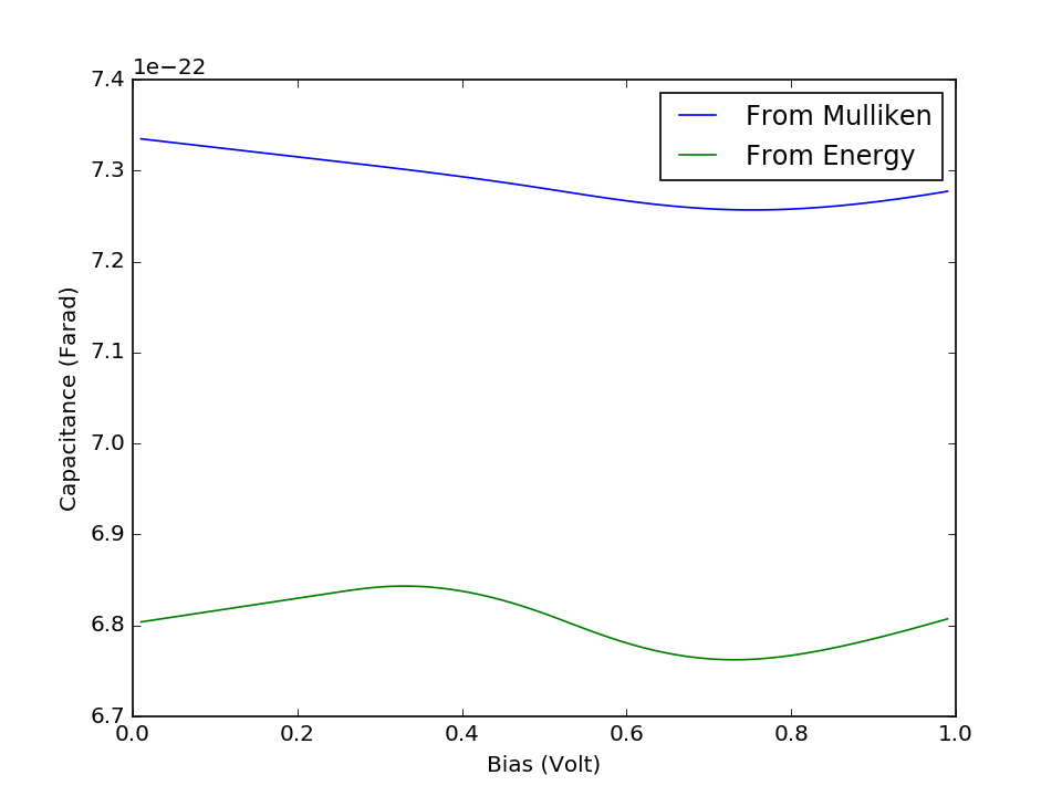
Attention
The present example uses rather few data points to illustrate the method. In general, you should use more than five data points to get an accurate analysis.
Dielectric spacer material
The electric field in the vacuum gap is extremely high (over 900*106 V/m at 1 V bias) and would immediately lead to a breakdown discharge in the device. Replacing the vacuum gap between the capacitor plates with a dielectric material can partly solve this.
There are two different ways to do this using QuantumATK:
Insert a dielectric material, and explicitly form the two metal–semiconductor–metal interfaces:
Spatial region: Use the QuantumATK Builder to place a dielectric spatial region between the surfaces.
Use a cheaper and less rigorous approach, where you simply modify the dielectric constant of the region between the gold surfaces:
Implicit solvent method: Assign a dielectric constant different than 1 to the vacuum region by modifying settings in the Poisson solver.
For demonstration purposes, we here go for the first option.
Note
In both cases it is necessary to use the Multigrid Poisson solver,
but you can still have periodic boundary conditions along A and B.
Dielectric spatial region
Follow the steps that led to calculation of the capacitance
from electrostatic energy analysis, but add the dielectric spatial region
and change the Poisson solver to Multigrid.
To use a dielectric spatial region, go to the
Builder and use the
tool to place
between the surfaces a box with a relative dielectric constant of 10:

Note
The dielectric region is a rectangular box, while the unit cell is hexagonal for the present [111] fcc surface. To solve the mismatch, make sure the rectangular box is large enough in the AB plane to extend outside the unit cell. The parts outside the cell will be cut off during the calculation.
Then send the new geometry to the Script Generator
and repeat all the steps. Or simply open the structure in the Editor
 and copy/paste the relevant parts of the scripts you
already have, and change the names of the output files.
and copy/paste the relevant parts of the scripts you
already have, and change the names of the output files.
The results are illustrated below. The position of the dielectric region is indicated by the grey shading. You can clearly see the expected discontinuity of the electric field near the edges of the dielectric region, and you will find that the capacitance has significantly increased.
Note
The scripts used in the electrostatic energy analysis are self-contained and generic. They can be used to analyse other systems as well, after suitable modification of the file names.
The scripts used in the Mulliken charge analysis need to be modified before they can be used for other systems, to account for geometry changes.
These approaches are valid only if the current through the device is very small. For example, the transmission is extremely small (it’s a capacitor – not a diode!). You can verify that the transmission is extremely small for this large vacuum gap, of the order 10-23.
Tip
What next? Another interesting example of a nano-scale capacitor would be a one formed by Carbon Nanotube Junctions.