Spin-orbit splitting of semiconductor band structures
The spin-orbit coupling (SOC) is a relativistic effect that causes splitting of the electronic bands in many materials, including semiconductors. This effect is not included in standard calculations.
In this tutorial, you will learn how to take spin-orbit coupling into account in density functional theory calculations (ATK-DFT) and also in semi-empirical Slater-Koster calculations (ATK-SE) for semiconductors.
Outline
We start off with a short introduction to relativistic effetcs in electronic structure theory, including spin-orbit coupling.
You will then use ATK-DFT to study how the SOC splits the electronic bands of Silicon around the \(\Gamma\)-point, leading to the so-called “split-off” valence band and bands with “heavy” and “light” holes.
You will then employ a SO+MGGA method to get not only the correct band splits but also a reliable estimate of the indirect band gap.
Lastly, you will consider the gallium-arsenide crystal, and use the Slater–Koster method with SOC parameters to compute the GaAs band structure.
Relavistic effects in Kohn-Sham DFT
The standard time-independent Kohn-Sham Hamiltonian describes non-relativistic electrons moving in an external field set up by atomic nuclei (and possibly any other external time-independent fields). Relavistic effects are therefore completely disregarded. This is usually a very good approximation for valence electrons outside the atomic cores, but for heavy elements, like gold and lead, relativistic contributions to the electronic structure can be crucial. Moreover, spin-orbit coupling, which cannot be captured in a strictly non-relativistic description, will often break degeneracy in solid band dispersions, and thereby lead to experimentally observed band splittings.
Electronic-structure software employing pseudopotentials, like the ATK-DFT engine does, will usually incorporate relativistic effects on core electrons in an approximate manner by using scalar-relativistic pseudopotentials. This is a computationally efficient and quite reliable approach.
However, calculations including spin-orbit coupling require fully relativistic pseudopotentials and a noncollinear representation of the electronic spin degrees of freedom. This can be computationally intense, but is mandatory if relativistic effects on the electronic ground state are to be taken fully into account.
Silicon band splitting with ATK-DFT
You will now use ATK-DFT to calculate the LDA bandstructure of silicon with and without spin-orbit coupling.
Note
Spin-orbit DFT calculations are more expensive than standard LDA or GGA methods and will often require more SCF iterations to converge. Usually, it is therefore more efficient to first do a spin-polarized ground state calculation, and then use this state as an initial guess for the spin-orbit DFT calculation. This procedure reduces the number of spin-orbit SCF steps and significantly reduces the overall computational time.
Warning
Not all pseudopotentials can be used for spin-orbit DFT calculations. The OMX potentials supplied with QuantumATK contain the required SO terms, while the FHI potentials do not.
Hint
Please remember that OMX pseudopotentials have in general more valence electrons in the cores than the FHI potentials do. Therefore, the OMX potentials usually require good basis sets and higher density-mesh cutoff energies (e.g. 200 Hartree).
Use the Builder
 to set up the silicon crystal
with the default (experimental) lattice constant.
to set up the silicon crystal
with the default (experimental) lattice constant.Send the bulk configuration to the Script Generator
 and add two sets of the following three blocks:
 New Calculator,
  Initial State,
and
Initial State,
and  Bandstructure.

LSDA initial guess for the ground state
Double-click the first
New Calculator block,
and make the following changes to it:Select the OMX pseudopotential with 4 valence electrons, and use the “Medium” accuracy basis set:

In the Basic calculator settings, increase the density-mesh cutoff to 150 Hartree, select “Polarized” spin, set up a 7x7x7 k-point grid, and use
lsda.ncas output file:

Click OK to close the widget.
Double-click the first
Initial State block,
and set up an initial guess for spin polarization
of the silicon crystal:Change Initial state type to “User spin”. Then click OK.

Note
This defines a non-zero initial guess for the silicon polarization, even though we know that silicon is not magnetic. Indeed, we will find that it is not, because the self-consistent polarization will be close to zero. However, a self-consist LSDA calculation is usually a good starting point for noncollinear calculation, with or withour spin-orbit.
Edit the first
Bandstructure block,
such that it maps out the \(L-\Gamma-X\) path
with 50 points per segment, and saves the data in the
lsda.ncfile:
That fully defines the LSDA ground state calculation followed by a band structure analysis.
SOLDA calculation
Next, you will set up a similar workflow for SOLDA calculations, but use the LSDA ground state as an initial guess for the SOLDA ground state.
Modify the second
New Calculator block
such that it is similar to the first one,
but choose the “Noncollinear Spin-Orbit” spin option
and save the results in so-lda.nc.Hint
Remember to also choose the correct basis set and pseudopotential.

In the second
Initial State block,
select “Use old calculation” and point to lsda.ncas the file from where to read the initial state:Warning
If you use a non-polarized calculation as initial state for the spin-orbit calculation, you should set the initial spin to zero.

Set up the last
Bandstructure block similarly to the first one,
and save the results in so-lda.nc: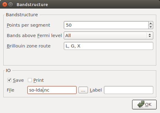
The ATK-DFT script is now done. It can also be downloaded from here:
lda.py.
Send the script to the Job Manager  ,
save it as
,
save it as lda.py, and run it in serial on your local machine.
It should take only a few minutes to finish.

You should be able to monitor the progress of the job while it is running:

Results
Once the results have appeared on the LabFloor, highlight the two bandstructure objects and use the Compare Data plugin to directly visualize the LSDA and SO+LDA band structures in the same plot:

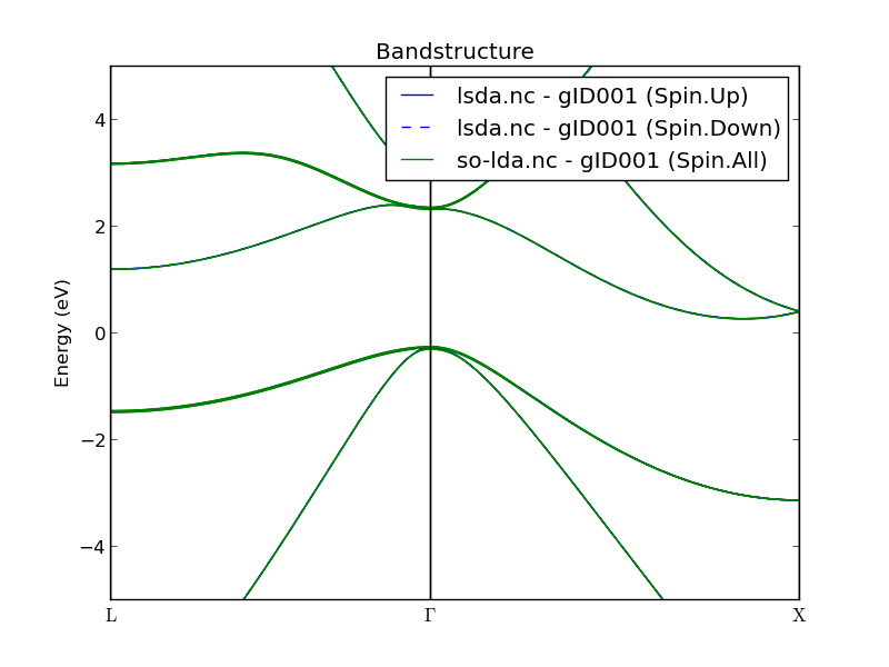
Fig. 30 Comparison of the LSDA (blue) and SOLDA (green) band structures of silicon.
Several observations can be made:
As expected, the LSDA spin-up and spin-down bands are identical (blue lines).
At first sight, SO+LDA and LSDA bands appear indistinguishable. In particular, they both yield and indirect band gap of around 0.5 eV.
However, if you zoom in around the highest valence bands at the \(\Gamma\)-point (see below), the SO coupling has partly lifted the degeneracy of those bands by splitting them:
The top band has split into two bands, corresponding to “heavy” and “light” holes.
The third band is now separated from the two others by the so-called “split-off” energy, experimentally measured to be 42.6 meV [1]. With SO+LDA we find 44 meV.

Fig. 31 Valence-band top at the silicon \(\Gamma\)-point calculated with LSDA (blue) and SOLDA (green). The latter leads to significant spin-orbit splitting of the bands, and predicts a split-off energy of 44 meV.
SO+MGGA band gap
The band splitting obtained above with the SO+LDA method is in very good agreement with the experimental splitting (42.6 meV [1]) However, the band gap is less than half of the experimental value (1.12 eV).
This is largely remedied by applying the TB09LDA method, which employs a meta-GGA exchange-correlation potential and gives remarkably accurate band gaps for semiconductors [2]. We should therefore expect the SO+MGGA method to accurately predict band splittings as well as band gaps.
Go back to the Script Generator and delete the first set of three blocks from the script.
Change the exchange correlation functional to “SOMGGA” and use
so-mgga.ncas output.Make sure that the Initial State block reads in the ground state from
lsda.nc, and that the Bandstructure analysis block saves its output inso-mgga.nc.Save the script as
mgga.py. You can also download it if needed:mgga.py.Run the job – it may take 5-10 minutes to finish if run in serial. This can be reduced to 3 minutes if the job is run in parallel with 4 MPI processes.
Tip
The scf convergence can for small bulk systems be speed-up by increasing the damping factor to 0.5 in the iteration control parameters setup.
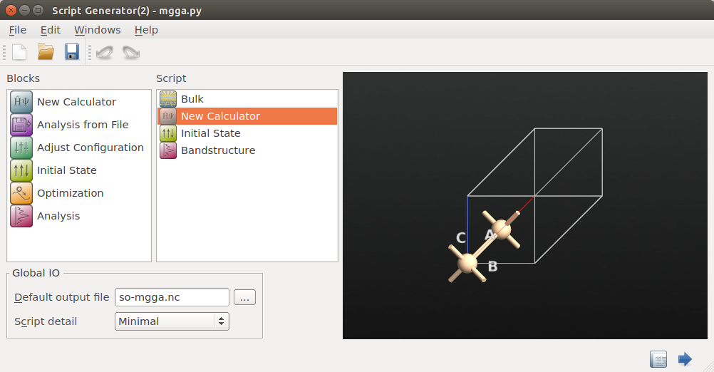
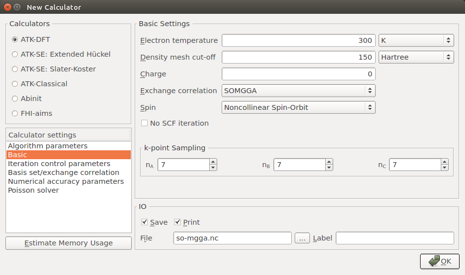
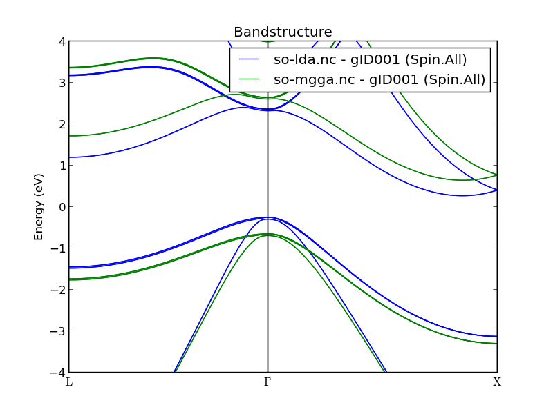
Fig. 32 Comparison of the SOLDA and SOMGGA bandstructures of silicon. The SOMGGA indirect band gap of 1.3 eV is close to experimental values.
Results
Using again the Compare Data plugin, you can now compare the SO+LDA band structure to the SO+MGGA one.
In the figure above it is clear that SO+MGGA has increased the distance from valence to conduction bands. Try to use the Bandstructure Analyzer plugin to measure the SO+MGGA indirect band gap. You should find ~1.3 eV.
The figure below zooms in on the split valence bands. They have not changed much from the SO+LDA results, apart from a vertical shift.
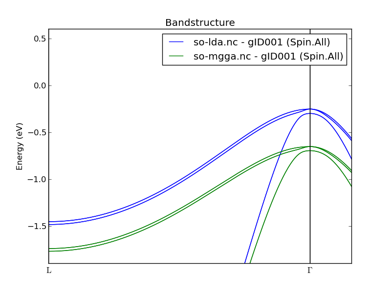
Fig. 33 Zoom-in on the split valence bands of silicon.
GaAs band structure with ATK-SE and SO coupling
The ATK-SE engine offers tight-binding models for electronic structure calculations as a parametrized alternative to DFT. The Slater–Koster (SK) model is one such method, and includes spin-orbit coupling through a speciel SOC parameter, which is implemented in the ATK-SE engine.
Use the Builder to create the GaAs bulk configuration
with experimental lattice constant, and use the Scripter
to set up the Slater–Koster calculation:
Add the
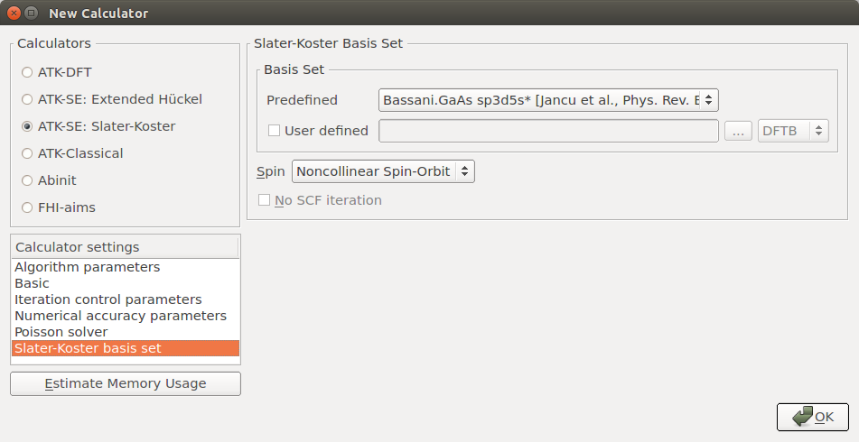
New Calculator and Bandstructure blocks.Choose the ATK-SE: Slater-Koster calculator engine and the Bassani.sp3d5s basis set, and choose Noncollinear Spin-Orbit for the spin.
In the Bandstructure block, increase the Points per segment to 101 in order to finely sample the band structure between each high-symmetry point, and trim the default Brillouin zone route such that it reads “G, X, W, L, G, K”.

Run the calculation – it will only take a few seconds – and then use the Bandstructure Analyzer to plot the results. The SO induced spin-splitting of the GaAs band structure is clearly visible. If you zoom in a bit you can measure a direct band gap of 1.51 eV at the \(\Gamma\)-point, which is virtually identical to the experimental gap at zero Kelvin.

Fig. 34 Slater–Koster spin-orbit band structure of GaAs.