Charged Point Defects

Defining defects
Introduction
The entry point to calculating charged point defect properties with QuantumATK is a set of objects called defect Generators. They generate a dictionary of abstract defect definitions (NamedPointDefect) based on the symmetry of the supplied reference or host BulkConfiguration.
Defect generator types
The defect generator types are:
VacancyGenerator for vacancy defects that remove an atom from the host lattice.
SubstitutionalGenerator for substitutional defects that replace an element in a lattice site.
InterstitialGenerator for interstitial defects occupying empty spaces between lattice sites. The positions that atoms can occupy are calculated using Voronoi geometry analysis. Atoms can be placed either on Voronoi vertices, faces or ridges.
SplitInterstitialGenerator for split interstitial defects. These are interstitial defects that make extra room by displacing a lattice atom out their site.
DefectPairGenerator for site defects paired with another point defect. This generator is constructed using the generators for the two point defects in the pair.
Defect generator usage
The defect generators always generate all possible defects of the selected type. Symmetrically equivalent defects are then sorted into groups that are assigned unique symmetry indices. Note that within each group the defects are sorted with respect to their distance to the unit cell center, the closest one being first.
After the initial generation, the defects can be filtered based on various selection criteria:
filterBySymmetryIndexis intended to pick particular defects by symmetry.filterByLatticeSpeciesis intended to select defects by the original element at the defect site.filterByPointDefectis intended to explicitly include or exclude defects in a provided list of defects.filterByDistinctConfigurationsuses a structural descriptor to select a number of the most distinct defect configurations.filterByZPositionIntervalpicks only those defects in the given z coordinate interval.
Pristine Reference Configuration
The PristineConfiguration is used to calculate all the reference data of the original, defect-free configuration. This is used in the point defect calculation to provide the reference material and its relevant properties, such as total energy and band gap. Parameters that are common in the calculation of many defects are also stored in the PristineConfiguration class. These include parameters such as the supercell size of the defect, the reference calculator and the type of charge correction to apply to the defect. In this way consistency can be assured when calculating a series of defects.
When calculating the band gap, the PristineConfiguration has the option to use a
different calculator specifically for the band gap. This can be useful where an appropriate
calculator for the band gap, such as the LCAOCalculator using HSE06, may be too
computationally expensive for calculating all of the defect properties for the series of defects.
While a supercell is often used for the defect calculation, the band gap is calculated using the
unit cell of the pristine material. This means the band gap calculator can be significantly more
computationally demanding than the reference energy calculator, as it is applied to a smaller
configuration.
Vibrational modes can also be optionally calculated for the pristine material. If calculated, the vibrational modes can be used to estimate the vibrational enthalpy and entropy of the material, which contributes to the formation free energy of the defect. As with the band gap a specific phonon calculator can be given as input. Typically this is used where another less computationally demanding calculator is known to give good estimates of the vibrational modes. This may be a Moment Tensor Potential (MTP) based TremoloXCalculator that was trained on the types of defects being studied. Calculating the vibrational modes in the pristine material will also enable calculating the same vibrational modes in the defect.
Charge Correction Schemes
In density functional theory (DFT) calculations the structure in the BulkConfiguration is considered to be the fundamental repeat unit of the extended material. Placing a defect in this structure implies that the defect is similarly repeated throughout the material, giving an artificially high concentration of defects. The problem is compounded when adding charges to the defect, as these charges are also repeated throughout the material. In DFT calculations this non-neutral charge is handled by adding a compensating background charge to the material. This conceptual difference between an isolated defect and a repeated periodic defect gives rise to some artifacts in the calculation that need to be corrected.
When performing accurate defect calculations it is first important to make sure that the defect configuration is large enough so that the atomic structure around the defect is not effected by its repeated copies. This applies to both charged and neutral defects. This means that a supercell of the original pristine material is likely needed to remove structural interactions between defects.
In the case of charged defects the added background charge and periodic defect charges also need to be corrected. One method to do this is the scheme of Freysoldt, Neugebauer and Van de Walle (FNV) [FNVanDWalle09]. This correction is specified in the ChargedPointDefectConfiguration class by passing as input the IsotropicFiniteSizeCorrectionParameters class. In this method the corrections are separated into long-range and short range terms. The long range interactions between defects are modeled assuming a Gaussian model charge at the defect. Interactions between defects are then calculated via Ewald summation. A short-range correction is also made by comparing the model charge to the difference between the defect and pristine potentials. At distances far from the defect this should be constant. The average value of the potential difference then gives an additional alignment correction. Both of these corrections take into account the dielectric constant of the pristine material in determining the electrostatic energies.
Using this correction scheme the formation energy of the defect at a given charge state \(E_f(X^q)\) can be given as:
(27)¶\[E_f(X^q) = E_{tot}(X^q) - E_{bulk} - \sum_i n_i\mu_i + q(E_F + \mu_e + \delta_{q/b}) - E_{lat}^q\]
Here \(E_{tot}\) gives the DFT energy of the defect and pristine bulk materials respectively, \(\mu_i\) is the chemical potential of each element, \(n_i\) is the change in the number of each element, \(E_F\) is the Fermi energy, \(\mu_e\) is the electronic chemical potential \(\delta_{q/b}\) is the short range potential correction term and \(E_{lat}^q\) is the long range correction term. The Fermi energy is set to the reference for the chemical potential, generally the valence band maximum. The addition of the electronic chemical potential allows for modeling changes in the Fermi level due to doping or other causes.
In addition to electronic corrections an additional finite size correction can be added to correct for a change in stress [FGH+14]. Adding a defect to the periodic unit cell adds additional stress to the structure. In the isolated defect this stress is normally dissipated in the surrounding pristine material. Given the bulk modulus of the pristine material \(B\), the additional correction due to elastic interactions can be estimated as:
Here \(V\) is the volume of the defect unit cell and \(P-P_0\) is the difference in pressure calculated in the defect and pristine materials.
Chemical Potentials in Compound Materials
Defects in materials often exist in equilibrium with other materials. These materials can be the reservoir for the defect elements. For the formation energy to correctly reflect the equilibrium of elements in defects and in their respective reservoir, the energy of the atoms in this reservoir needs to be included. This is done by calculating the chemical potential of each element in the defect. Using this, the change in free energy between the reference state and the defect can be calculated. For compound materials, the total energy of a compound material is always smaller than the sum of the chemical potentials of the individual elements.
In the defect framework there are two ways to specify a chemical potential for an element. The first way is to calculate the atomic energy based on calculations of a suitable elemental reference material. This is done through the CalculatedChemicalPotential class. The choice of this material may be influenced by the kind of element reservoir that may be present in the device. In these calculations the atomic energy is simply defined as the average energy of an atom. This energy includes both the energy required to form a single atom, as well as the formation energy required to form the reference material. Optionally vibrational energies can also be included, so that an entropy per atom can also be calculated. Potentials defined in this way can be used to model element rich environments for defects. For instance in silicon carbide, if the chemical potential for silicon is defined in this way it models a silicon rich environment, where bulk silicon acts as the reservoir for silicon. If all elements are defined in this way it gives elemental reference conditions. Here the total energy of the material is given as the sum of the atomic chemical potentials and the heat of formation. In silicon carbide this leads to the expression:
Here \(dH\) is the heat of formation and \(\mu^e\) is the elemental chemical potential. In this reference state it is assumed that each element can be exchanged with a corresponding elemental reservoir.
In addition to calculating the chemical potential, the chemical potential can also be directly specified using the ReferenceChemicalPotential class. Here the entropy and enthalpy of the element can be specified for a specific temperature. Note that the enthalpy here must include the energy of forming an isolated atom, as well the the reservoir formation energy. Using this definition of the chemical potential it is possible to provide other reference environments. One possible reference environment is the heat of formation reference conditions. Here the heat of formation of the material is evenly distributed among the available atoms. This assumes that each element is exchanged with a reservoir of the same materials as the defect. In silicon carbide the silicon heat of formation chemical potential \(\mu^f\) would then be:
A third possible reference for specific element rich environments would be to assume the potential for the rich element is the elemental potential. The heat of formation for the material is then distributed to the remaining elements. This assumes that one element is exchanged with an element specific reservoir, whereas the other elements are exchanged with the host material. This gives a poor environment for the other elements that do not have their own reservoir. In silicon carbide the carbon poor chemical potential \(\mu_C^p\) in a silicon rich environment can be given as:
Charged Point Defect Calculation
The charged point defect structure and its properties is calculated with the
ChargedPointDefectConfiguration object. This object requires a pristine configuration,
a defect definition and a sequence of atomic chemical potentials for the elements in the defect.
The calculation of the defect is started by calling the update method on the object. Once
the defect calculation is complete a number of methods on the object are available for querying the
results of the calculation. These include the optimized defect configuration, symmetrically
equivalent representations of the defect, the defect formation energy and concentration and the
electron trap levels of the defect. Alternatively the defect calculation can be analyzed in the
Charged Point Defect Analyzer.
Defining defects
The definition of a defect required for the ChargedPointDefectConfiguration object is a NamedPointDefect. These can be generated for a specific host configuration using the defect generators.
Defect Relaxation
In the ChargedPointDefectConfiguration object there are two independent relaxation cycles that can be enabled or disabled. This allows doing relaxation away from the minimum with a computationally cheaper method, such as an MTP, and then fully relaxing the structure with the appropriate reference calculator. The first is a pre-relaxation step. This takes a separate pre-relaxation calculator and optionally a OptimizeGeometryParameters. The second step is a relaxation step, which is performed with the reference energy calculator. A separate OptimizeGeometryParameters can also be given for this stage. Note that during the relaxation it is not possible to relax the cell, as the cell size is set by the pristine material.
During optimization the charge state closest to zero is performed first. This step always performs the requested pre-relaxation and relaxation steps. The subsequent charge state relaxations are then started from the nearest relaxed charge state. If a TremoloXCalculator is given as the pre-relaxation calculator this step is ignored, as these calculators cannot model different charge states. For other calculators the pre-relaxation step, if enabled, is performed before the relaxation step.
To stop the defect structure from possibly drifting during the relaxation, it can be beneficial to fix an atom during optimization. The atom selected to be fixed is one of the atoms furthest from the defect, so that the defect itself is able to fully relax. Adding small random displacements to the initial configuration can also aid optimization in breaking symmetry and moving it off potential saddle points.
Formation energy
The formation energy is a measure of the energy required to create the defect in the given host material using the defined atomic reservoirs. The formation energy also depends on the charge state, the temperature and the electronic chemical potential. The general formula for the defect formation internal electronic energy is given in equation (27). Adding vibrational modes to the calculation also adds vibrational internal energy and entropy contributions. In this case the total formation free energy \(\delta H_f\) is given as:
Without vibrational corrections the formation free energy is calculated as the change in the electronic formation internal energy.
The formation free energy is calculated using the formationFreeEnergy method on the
ChargedPointDefectConfiguration object. This method has a number of options depending on the
specifics of the defect. The electronic chemical potential can be specified with the argument
electronic_chemical_potential. The reference for the electronic chemical potential can also
be given with the electronic_chemical_potential_reference. Here the reference for the electronic
chemical potential can be either the valence band edge or the conduction band edge. In cases where
a different band gap calculator was used, the energy of charged defects needs to be corrected for
the different band gap. The alignment is specified the the defect_type argument. Here the defect
can be specified as a deep level defect, a shallow acceptor or a shallow donor. This changes
whether the defect energy is aligned with the Fermi level, valence band maximum or conduction band
minimum respectively. Finally the vibrational corrections, where available, can be included or
excluded with the argument include_vibrations.
Defect Concentration
Where defects are in equilibrium with the surrounding atomic reservoirs, the concentration of the
defect is directly related to the formation energy. The concentration of a defect \(X\) in
charge state \(q\) can be calculated with the concentration method using the
following equation (see also [Meh07b]):
where
\(n\) is the number of defect sites in the supercell.
\(V\) is the volume of the supercell.
\(\theta\) is the number of internal degree of freedom, for example, the number of possible spin states.
\(S^f_{X^q}\) is the vibrational formation entropy.
\(k_B\) is the Boltzmann constant.
\(E^f_{X^q}\) is the formation internal energy.
\(T\) is the Temperature.
One can also obtain the intrinsic concentration with the intrinsicConcentration method which is
just the sum of the concentrations of all charge states available on
the ChargedPointDefectConfiguration.
Symmetry of the Defect
In each point defect calculation the symmetry of the defect is analyzed. Here the symmetry
operations of the original pristine material are used to determine the symmetrically equivalent
defect structures, as well as the number of symmetry operations that produce each defect
configuration. This can be useful for identifying if two seemingly different defects are actually
symmetrically equivalent representations of the same defect. The symmetrically equivalent defect
configurations can be accessed using the symmetricDefect method on the
ChargedPointDefectConfiguration object. For each defect configuration the center of the
defect is also calculated by calculated the center of the modified atoms in the defect material.
The symmetrically equivalent positions of the the defect can also be accessed using the
symmetricDefectPosition method.
When deciding the supercell repetitions of the pristine material for the defect, it is important to preserve the Bravais lattice symmetry of the pristine material. Breaking the symmetry of the Bravais lattice by providing different numbers of repetitions in symmetrically equivalent directions can produce materials with different symmetry, breaking the validity of the symmetry analysis. Such repetitions can also introduce directional artifacts in the calculation. As an example, bulk silicon has a simple cubic conventional Bravais lattice. Here each direction is symmetrically equivalent. Using 1x2x3 repetitions to create the defect supercell breaks this Bravais lattice type, as now each direction is not equivalent. There is a different distance to the repeated defect in each direction. Using a 2x2x2 defect repetition maintains the Bravais lattice symmetry, as there is still an equivalent distance to the repeated defect in each direction. Breaking the Bravais lattice symmetry can also cause the detection of symmetrically equivalent transition paths to fail.
Ghost atoms
The basis set used in the DFT calculations depends on the atoms included. In the case of vacancy defects, this means that the basis set functions centered on the defect are normally removed when the defect is calculated. This can lead to errors in the energy in cases where the surrounding atoms are stabilized by basis functions belonging to the vacancy site atom. To alleviate this problem a ghost atom can be placed at the defect site during the defect DFT calculations. This maintains the full basis set from the pristine material, allowing a more direct comparison. In geometry optimizations the ghost atom is kept at the vacancy defect center.
Ghost atoms are only supported for vacancy defects. Ghost atoms also cannot be used when calculating transition paths. This is because the ghost atom cannot be included in the transition state. For other defects basis functions are added as well as removed, and so the same basis set cannot be re-created with ghost atoms. In these cases increasing the basis set size can give more accurate defect energies as it reduces the dependence of the energy on specific basis functions.
Interfaces and amorphous materials
Modeling defects at interfaces and in amorphous materials brings additional challenges. These
materials often have low or no symmetry, meaning that in each configuration a large number of
different defects may be possible. In the defect generators there are two specific methods that are
useful for filtering defects in low symmetry configurations. The first method,
filterByZPositionInterval allows selecting defects in a particular slice along the C direction.
The enables selecting defects at a particular depth at the interface. Secondly, the method
filterByDistinctConfigurations allows selecting for the most diverse set of defects up to a
certain number in a set of defects. It does this by assigning similarity scores using atom-based
descriptors [SGS+13]. This can reduce the number of possible defects while still
spanning the space of possible defects.
Another difficulty with calculating defects at interfaces is with the charge correction. This correction assumes an isotropic material. At interfaces, especially where there is a significant change in the dielectric constants between the two materials, this correction may break down. This is a problem for accurate formation energies of charged point defects. Neutral defects do not require the same energy correction.
Analyzing charged point defect calculations
The results of charged point defect calculations can be analyzed in the Charged Point Defect Analyzer.
Opening defects in the analyzer
The analyzer can be opened by double-clicking on a ChargedPointDefectConfiguration object in the Data Tool. Multiple defects can be opened in the analyzer by selecting the defects and right-clicking to bring up the context menu, and then selecting to open in the analyzer. New defects can be easily added by dragging them onto the Defects collection in the Defects tab. Once loaded into the analyzer the defects can be renamed by clicking on the name. Allowing multiple defects to be loaded into the analyzer makes it simple to compare the results of calculations on different defects. Defect calculations that only differ in the supercell size can also be merged into one defect record in the analyzer. This is most useful for comparing the scaling behavior of the formation energy with defect supercell size.
An example results file can be downloaded here. This file
contains two vacancy defects in SiC calculated with LCAO-PBE. These defects can be opened in the
analyzer.
Comparing defect configurations
In the Compare tab the configurations of two different defects can be shown and inspected. This allows easy visualization of the two defect structures, so that similarities and differences between different defects can be observed. In the analyzer the symmetry representation and unit cell translation within the supercell can be selected. Using these it is possible to visually see if two defects are symmetrically equivalent. This is most useful in the case of interstitial defects, where defects starting from different positions may relax into common structures.
Analyzing trap levels
Trap levels can be analyzed in both the Formation Energy and Trap Levels tabs. In the Formation Energy tab the change in formation Helmholtz energy with electronic chemical potential is plotted for each charge state. The intersections between these lines show the trap levels in the defect. Optionally the lowest stable charge state (SCS) can also be plotted. Different temperatures can be given at which to plot the formation Helmholtz energy. The finite size corrections can also be added or removed from the plotted formation energy. In the plot the valence and conduction bands are also show with blue shaded areas, showing whether or not the trap levels occur in the band gap.
The following plot shows a typical result for a defect calculation in silicon carbide. Here the -2 to +2 charge states are calculated, giving 4 stable transitions shown by the dashed lines. The intersections showing unstable transitions are also marked with a circle.
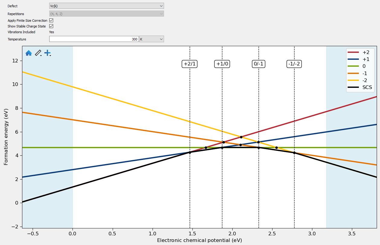
Fig. 231 Plot showing the formation energies of a carbon vacancy in silicon carbide.
In the Trap Levels tab the trap levels can also be directly plotted for each defect. This allows direct comparison of the trap levels for different defects. Here the relevant supercell size can be selected. Selecting a specific supercell size will show the trap levels of defects with that specific supercell size. Selecting largest will show the trap levels of the largest supercell size for each defect. As with the formation energy, different temperatures can be given and the finite size effects added or removed. It is also to plot both the stable transitions and unstable integer transitions. Unstable transitions are shown in dashed lines.
The following plot shows a typical result for a defect calculation in silicon carbide. Here the -2 to +2 charge states are calculated for a carbon vacancy at both the h and k sites.
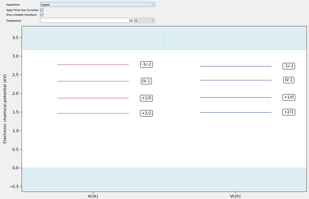
Fig. 232 Plot showing the trap levels of carbon vacancies in silicon carbide.
Analyzing defect concentrations
In the Concentration tab the concentration of each defect can be plotted with respect to temperature. The intrinsic concentration, which takes into account the concentration of each charge state, is also shown. A temperature range and number of steps can be given to set the temperatures of interest. The relevant electronic chemical potential at which to calculate the concentration can also be given. The concentrations can either be plotted in temperature / concentration or inverse temperature / log concentration units. The latter is often more useful for showing large differences in concentration between defects. In this plot a fit of the data to the Arrhenius equation is also shown.
The following plot shows the calculated concentrations of a carbon vacancy in silicon carbide plotted in inverse temperature / log concentration units. Here the electronic chemical potential set to the mid-gap level.
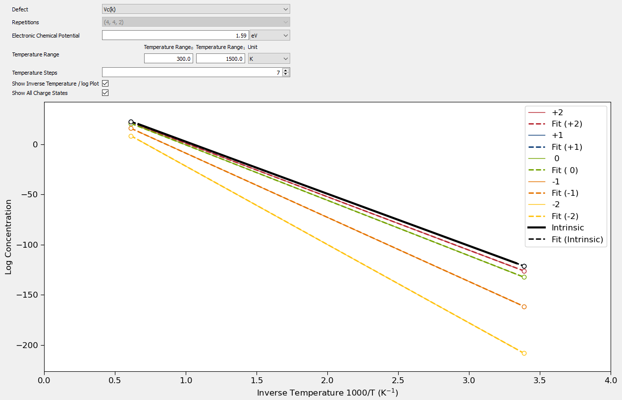
Fig. 233 Plot showing the concentrations of each charge state and the intrinsic concentration of a carbon vacancy in silicon carbide.
Checking the validity of charge corrections
When applying a charge correction to the defect formation energy it can be important to check the validity of the approximations in the correction for the individual defect charge states. In the case of the FNV correction it is assumed that the material is isotropic, and that the charge is located primarily at the defect site. The validity of the charge correction can be inspected using the Charged Point Defect Analyzer. By clicking on the Band Shift Correction tab you can inspect the value of the short range potential away from the defect. This potential should plateau at the correction value. By calculating the defect at different sizes it is also possible to check the scaling behavior of the defect. The short range potential scales in general as \(1/L^3\) while the long range correction scales as \(1/L\). If the correction is applied correctly extrapolating the formation energy out to infinite size should give the same formation energy. This can be inspected in the analyzer by selecting the Finite Size Scaling tab.
The following plots show some examples of calculations of carbon vacancies in silicon carbide. In the first figure a plot of the defect potential and the Gaussian correction potential is shown. Note that at larger distances from the defect in the middle of the plot, the differences between these two potentials is constant. This indicates that the Gaussian charge distribution is effectively correcting the potential from the defect at long range. The value of the potential here also gives the short range correction for the defect formation energy. In the second plot the scaling of the formation energy with system size is shown. Note that at the extrapolated infinite size, the corrected and uncorrected formation energies agree. This indicates that the corrections are able to effectively calculate the infinite size limit of the defect formation energy.
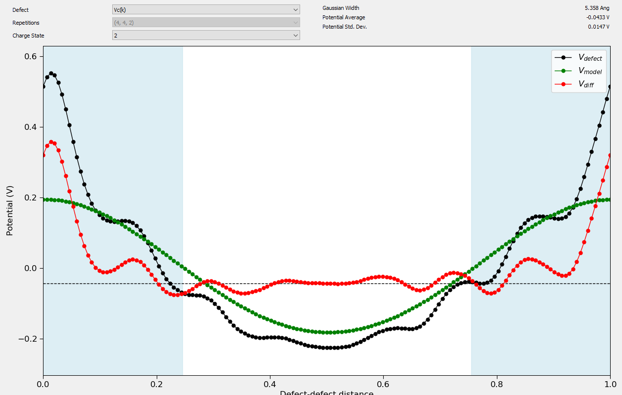
Fig. 234 Plot showing the defect potential correction for a +2 carbon vacancy in SiC. The flat potential away from the defect indicates that the short-range potential correction is valid for this defect.
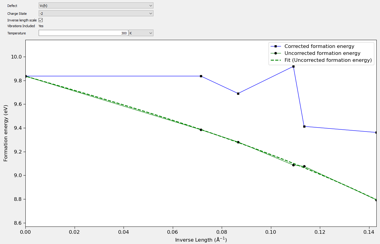
Fig. 235 Plot showing the convergence of the formation energy of a -2 carbon vacancy in SiC with defect supercell size. The convergence of the corrected and uncorrected energies at infinite size shows the corrections are effectively correcting the periodic effects in the defect calculation.
Viewing the defect report
In the Defect Report tab a textural representation of some information in the defect calculations can be generated. This includes data such as formation energies, concentrations and trap levels. In the analyzer the electronic chemical potential and temperature can be set at which to generate the information. This text output can be used as input for further analyses of the defects.
Defect migration
The migration of a defect within its host material is studied with the DefectMigrationPaths class. It takes as input two updated ChargedPointDefectConfiguration objects which will serve as the initial and final state of the transition. The object will calculate all possible transitions between the geometry optimized defects using their symmetry information. Optionally, the minimum and maximum travel distance may be specified.
The migration paths are obtained in the form of NudgedElasticBand configurations using the
generateNEBs method. The calculator should be set using the neb_calculator argument instead
of the setCalculator method of the NEB. This will make sure, numerical accuracy parameters stay
consistent for DFT calculators. If the default calculator is used, endpoint data (energies, forces,
stresses) will be taken from the defects, so they do not get re-calculated as part of the NEB, thus
saving time.
The NEBs are then optimized with OptimizeNudgedElasticBand. The endpoints need not be
optimized if the calculator is the same one used in ChargedPointDefectConfiguration,
unless the symmetry is broken by the choice of repetitions as this could lead to finite size
effects and structural artifacts. If the calculator was changed, e.g. when pre-optimizing with a
forcefield calculator, optimizing the endpoints may improve convergence of
the NudgedElasticBand. Since it is important for the accurate determination of migration
barriers to obtain a valid transition state, the climbing_image setting should always be set to
True.
Diffusivity of defects
In order to calculate the diffusivity of a certain defect, the optimized NudgedElasticBand and the two ChargedPointDefectConfiguration used to construct it need to be passed to the DefectDiffusivity class. It will then extract the transition state structure and calculate all data necessary such as the formation energy and vibrational corrections, if requested. These settings are taken from the input ChargedPointDefectConfiguration. Note that finite size corrections of the charge are currently not included in the diffusivity, since the position of the charge is ill-defined at the transition state.
To obtain the diffusivity for a defect \(X\) in charge state \(q\) one calls the
calculateDiffusivity method which implements the following equation
(see also [Meh07a]):
where
\(a\) is the migration/hopping distance.
\(d\) is the dimensionality of the diffusion.
\(Z\) is the number of adjacent sites to which the diffusion species can jump.
\(f\) is the correlation factor.
\(\nu_0\) is the attempt rate.
\(S^m_{X^q}\) is the migration entropy.
\(E^m_{X^q}\) is the migration energy.
The attempt rate \(\nu_0\) depends on the vibrational spectrum of the initial state \(\left\{\nu_i\right\}\) and the spectrum at the transition state \(\left\{ \nu'_i\right\}\):
The migration entropy is calculated as described in PhononDensityOfStates.
Analyzing Diffusion Results
The results of a DefectDiffusionRates calculation can be shown in the Defect Diffusion Rates Analyzer. This can be opened by simply double clicking on the corresponding results object in the Data Tool.
An example results file can be downloaded here. This file
contains the diffusion paths of Si and C vacancies in SiC. This was calculated with a Moment Tensor
Potential (MTP) that was trained on defects in SiC. This can be opened in the analyzer.
The Defect Diffusion Rates Analyzer shows information regarding the different calculated diffusion paths. The figure below shows the analyzer with data from calculations on silicon and carbon vacancies in silicon carbide.
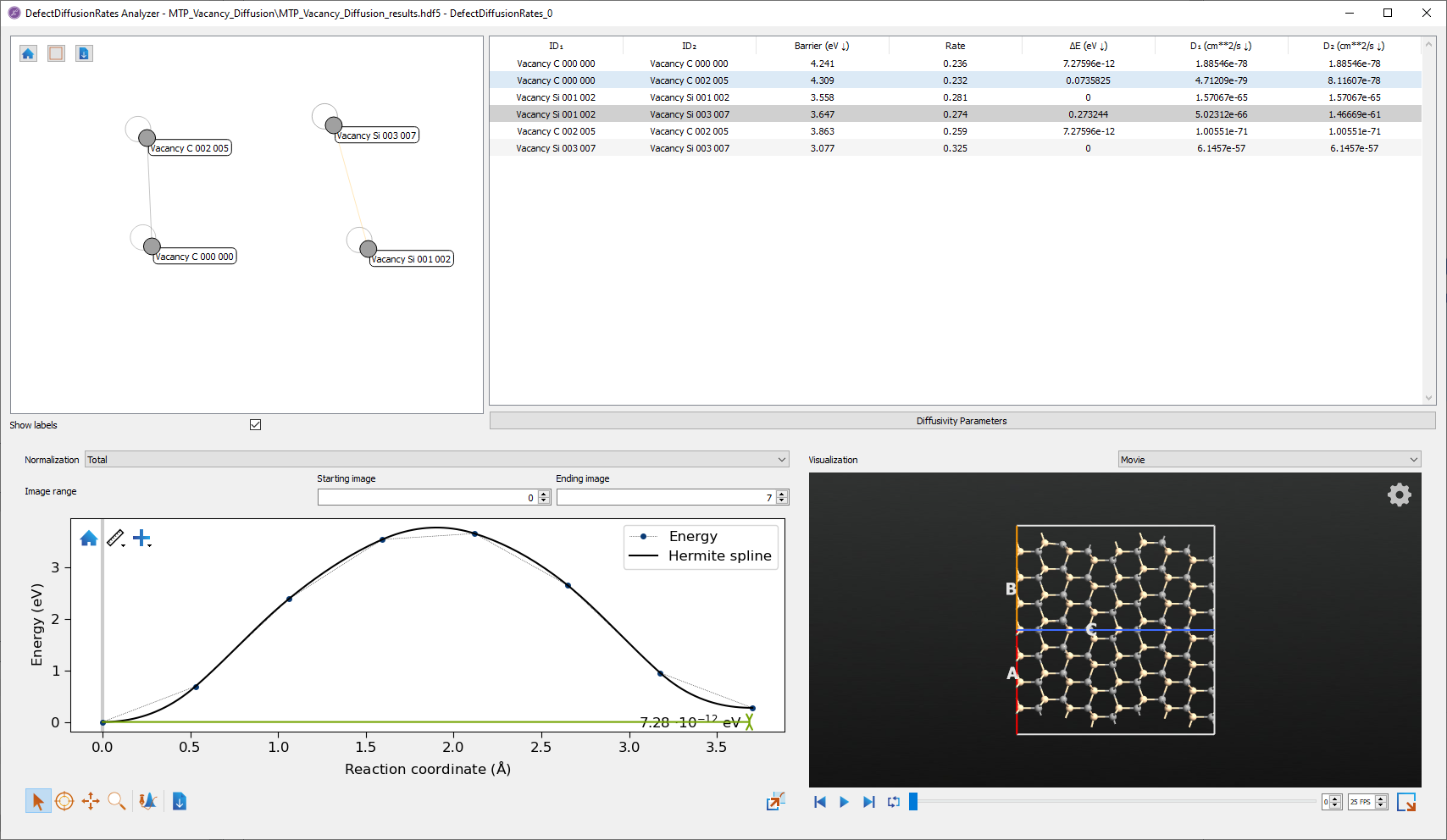
Fig. 236 The Defect Diffusion Rates Analyzer with data from calculations on vacancy diffusion in SiC.
In the top left panel is a graph view of the diffusion network. Here, each defect is shown as a filled circle. The lines indicate possible transitions between defects. The open circles represent self diffusion paths, where one defect transitions to the same type of defect at a different site. Depending on the defects selected, there can be one or more isolated graphs showing the connections between defects. In the example, as carbon vacancies cannot transition to silicon vacancies, two isolated graphs are shown.
In the a panel shows information about each defect diffusion path. This shows the forward reaction barrier, the forward transition energy, and the forward and reverse diffusivities for each transition path. These numbers can be used for further calculations on the defect dynamics, such as kinetic Monte Carlo simulations. The parameters used to calculate the diffusivity can be accessed and modified by pushing the Diffusivity Parameters button. This data can also be exported to CSV or XLSX format by right clicking on the panel.
At the bottom of the analyzer is shown the NEB for the selected defect transitions. Transitions can be selected by selecting either one of the transition lines in the transition graph, or selecting the corresponding data row in the data table. Visualizing the NEB allows inspecting the transition path and the likely transition state.
Christoph Freysoldt, Blazej Grabowski, Tilmann Hickel, Jörg Neugebauer, Georg Kresse, Anderson Janotti, and Chris G. Van De Walle. First-principles calculations for point defects in solids. Rev. Mod. Phys., 86(1):253–305, 2014. doi:10.1103/RevModPhys.86.253.
Christoph Freysoldt, Jörg Neugebauer, and Chris G. Van De Walle. Fully Ab Initio finite-size corrections for charged-defect supercell calculations. Phys. Rev. Lett., 102:016402, 2009. doi:10.1103/PhysRevLett.102.016402.
Helmut Mehrer. Dependence of Diffusion on Temperature and Pressure, pages 127–149. Springer, 2007.
Helmut Mehrer. Point Defects in Crystals, pages 69–91. Springer, 2007.
Ali Sadeghi, S. Alireza Ghasemi, Bastian Schaefer, Stephan Mohr, Markus A. Lill, and Stefan Goedecker. Metrics for measuring distances in configuration spaces. J. Chem. Phys, 139:184118, 2013. URL: https://doi.org/10.1063/1.4828704, doi:10.1063/1.4828704.