Transport in graphene nanoribbons
Version: 2016.0
Research on fundamental aspects and device applications of graphene is a very active field. This tutorial illustrates how QuantumATK can be utilized to study various applications related to graphene nanoribbons, ranging from a simple, infinite sheet of graphene to more complex junctions.
The main purpose of the tutorial is to demonstrate the basic work-flow in QuantumATK, how to build systems with nanoribbons and compute fundamental quantities such as band structures and transmission spectra using QuantumATK.
Introduction
The geometry of graphene is simple and regular, and the infinite, planar structure can easily be created, either by hand or by taking a single layer from the crystal structure of graphite.
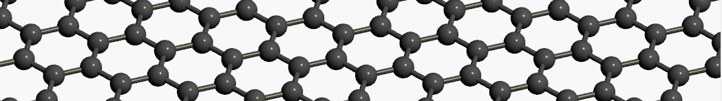
Fig. 83 A graphene sheet.
However, to create a device-like structure, the infinite sheet must be cut into a suitable shape. A common shape for electronics applications is a so-called graphene nanoribbon (GNR). These can be quite cumbersome to set up in an effective manner, not least considering the hydrogen passivation of the edges, which is needed in finite structures in order to satisfy all carbon valence electron bonds.
QuantumATK has a specific graphene nanoribbon Builder tool, and you will in this tutorial learn how to use it, and how to customize the structures it produces to make more advanced shapes of graphene. This will allow you to
calculate the band structure of ideal, infinite graphene nanoribbons, of either armchair or zigzag type, as a function of the ribbon width;
introduce doping or defects, on the edge or elsewhere, and study the influence on the transmission spectrum;
use basic ribbons as building blocks for your own device ideas, such as e.g. Z-shaped nanoribbon junctions.
This tutorial will show examples of each type of system.
Band structure of 2D graphene
Before starting with the nanoribbons, you will do a quick introductory calculation of the band structure of an infinite 2D sheet of graphene. This will also serve as a way to refresh the basic concepts and work flow in QuantumATK.
Constructing the graphene
Start QuantumATK, create a new project and give it a name, then select it and click Open. Launch the builder by clicking
the  Builder icon on the tool bar.
Graphene, and many other crystals, molecules and fullerenes, are available in the built-in database in QuantumATK. In the Builder, click and locate Graphene (while you are typing, you will see that graphite is included in the database too).
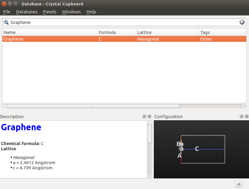
Double-click the line to add the structure to the Stash, or click the  in the lower right-hand corner.
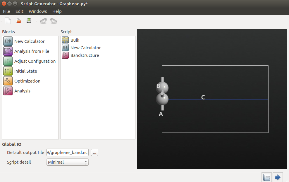
Now send the structure to the  Script Generator by clicking the
  “Send To” icon in the lower right-hand corner of the window.
Band structure: k-point sampling
You will now set up the band structure calculation. It is instructional for this particular system to compare the results of a DFT calculation with the semi-empirical method; as you will see, they are very similar.
The first step is to use the Extended Hückel method in the ATK-SE calculator to determine the required k-point sampling. Using this faster method saves time compared to doing the same investigation with DFT. The results should, for this aspect, be very similar.
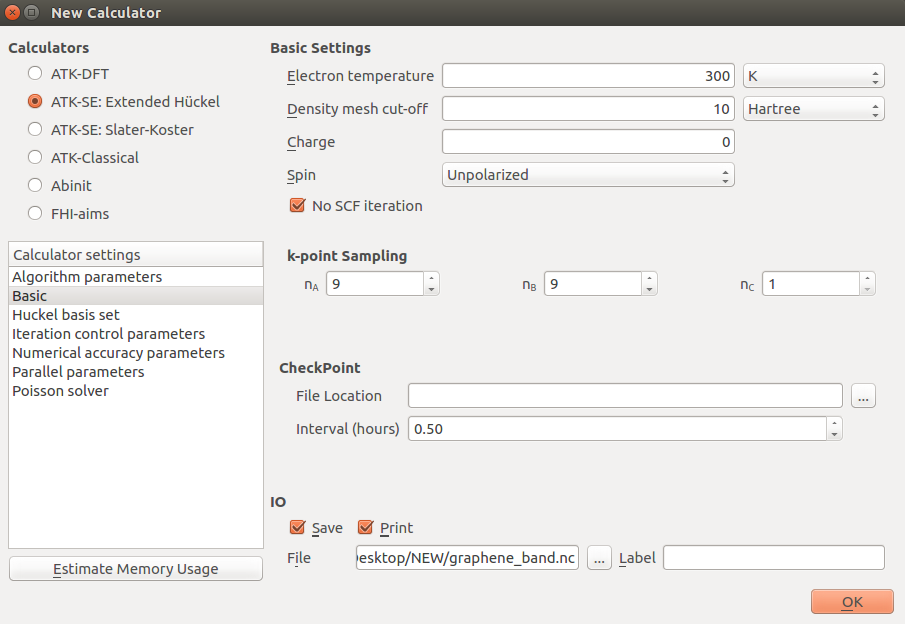
In the Script Generator, change the default output file to graphene_band.hdf5 and
add the following blocks to the script:
 New Calculator
 Bandstructure
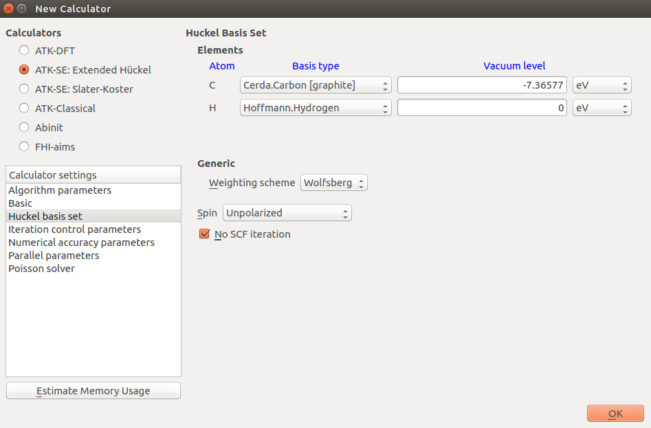
You should the default parameters, except the for the Hückel basis set parameters: Open the New Calculator by double-clicking it.
Select the “ATK-SE: Extended Hückel” calculator.
Under Huckel basis set, select the “Cerda.Carbon [graphite]” basis set.
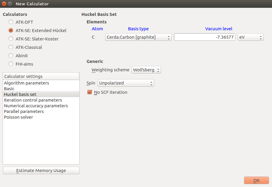
Make sure to use this basis set whenever studying graphene (or carbon nanotubes) with the extended Hückel method. Close the dialogue by clicking OK in the lower right-hand corner.
Next, open the Bandstructure block. A pre-defined route in the Brillouin zone is set up,
corresponding to a three-dimensional hexagonal Bravais lattice. Leave it like that for now; this point will
be discussed below.
Note
The different components of the script inherit the global output file name. It is possible to specify a unique file name for each analysis block, but usually it makes most sense to collect all results in the same file.
You are now ready to run the calculation: Send the script to the  Job Manager by clicking
the “Send To” button and by selecting “Job Manager” in the menu that shows up.
Job Manager by clicking
the “Send To” button and by selecting “Job Manager” in the menu that shows up.
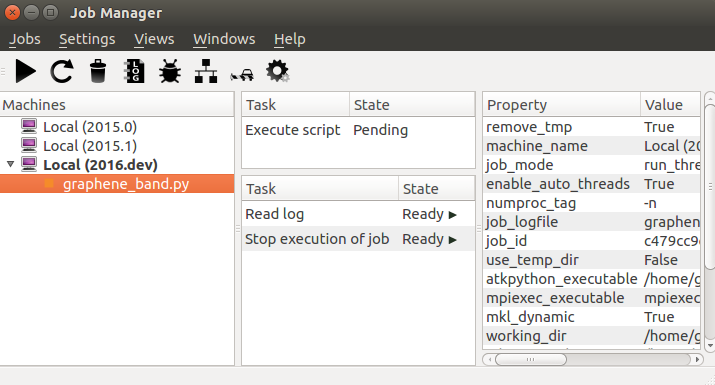
In the Job Manager, click  to run the job. The calculation takes only seconds to complete.
Analysis of the results
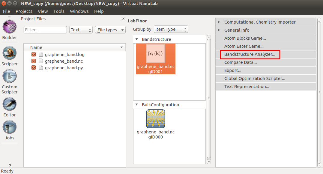
Once the calculation is finished, the graphene_band.hdf5 file should be visible in the Project Files list in QuantumATK.
On the LabFloor, select “Item Type” from the drop-down menu as shown in the below figure. Select the
Bandstructure item, and click the Bandstructure Analyzer button in the right-hand plugins panel.
The calculated band structure is visualized. However, on close inspection, you can see that is does not appear to be correct, since the Brillouin zone K point is supposed to coincide with the Fermi level.
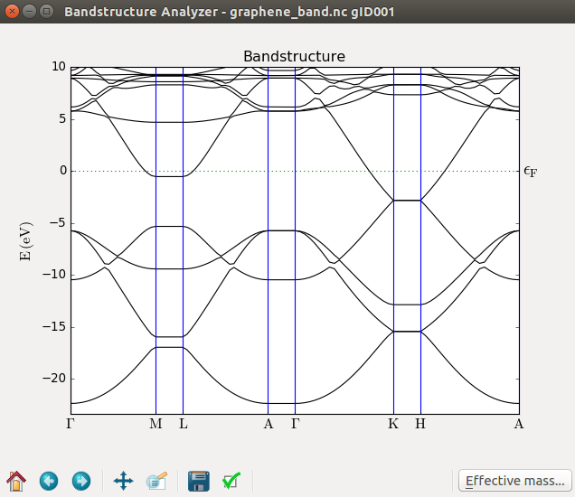
The cause of the poor band structure is insufficient k-point sampling; the default is to have just one point in each direction, and this fails to properly describe the graphene electronic structure.
Therefore, open the minimized Script Generator window again, open the Calculator
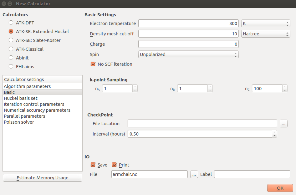
block, and enter 9x9x1 k-points under “Basic” settings.
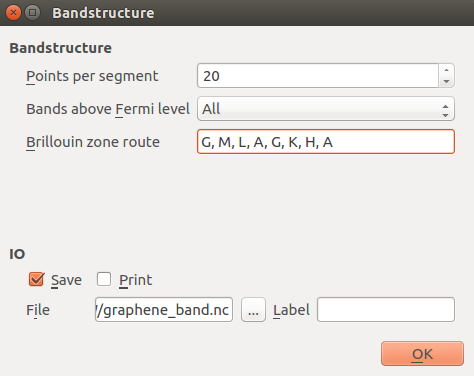
You should also adjust the symmetry points used for the band structure calculation to avoid the flat segments, which correspond to paths out of the planar graphene Brillouin zone. The only relevant k-points in a 2D hexagonal lattice are G=(0,0,0), K=(1/3,1/3,0), and M=(0,1/2,0), in units of the reciprocal lattice vectors.
This can easily be done in the Scripter (by double-clicking the Bandstructure block and editing the path), but to demonstrate how easy it is to use a script produced by the Script Generator as a template, you will now learn to do that by hand instead!
Send the script to the  Editor by clicking the icon in the Scripter. Locate the line
with the symmetry points, and edit it as shown below.
Editor by clicking the icon in the Scripter. Locate the line
with the symmetry points, and edit it as shown below.
bulk_configuration.setCalculator(calculator)
nlprint(bulk_configuration)
bulk_configuration.update()
nlsave('graphene_band.nc', bulk_configuration)

# -------------------------------------------------------------
# Bandstructure
# -------------------------------------------------------------
bandstructure = Bandstructure(
    configuration=bulk_configuration,
    route=['G', 'M', 'K', 'G'],
    points_per_segment=20,
    bands_above_fermi_level=All
    )
nlsave('graphene_band.nc', bandstructure)
Run the calculation by sending the script from the Editor to the Job Manager.
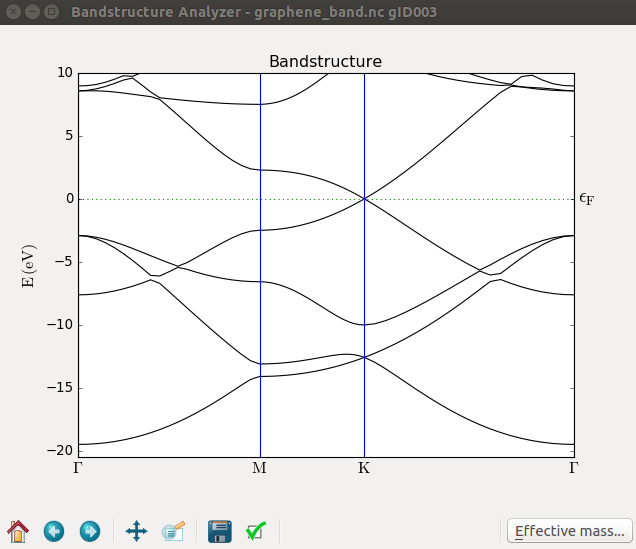
When the calculation finishes, a new Bandstructure object will be located on the LabFloor. Select it and plot it as
before. The Fermi level is now exactly at the K point, as illustrated below.
Calculate the band structure using DFT
You now know the required k-point sampling, and you can use this also for the DFT calculation. To switch method,
return to the Script Generator, open Calculator block, and select the ATK-DFT
calculator. Set the k-point sampling to 9x9x1, but leave all other parameters at their default values.
Tip
In case you closed the Script Generator window, you can reuse the geometry from the saved HDF5 file by dropping one of the bulk configuration inside it on the Scripter icon on the toolbar.
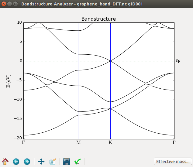
Keep again the same name for the output HDF5 file, and run the calculation. This will add yet another Bandstructure item to the LabFloor, which can be plotted like before. On inspection, you will find that the results are very similar to the Hückel band structure. The Hückel method therefore has good accuracy for this system and will be used for the further examples, mainly to save time; the interested reader is encouraged to verify that the results obtained with DFT are very similar.
Note
As it turns out, getting an accurate alignment of the K point to the Fermi level in graphene is not just a simple matter of having a lot of k-points. The results for 12x12x1 or 13x13x1 k-points are, for instance, considerably worse than those for 10x10x1. There is a general trend that more k-points are better, but on the other hand, 3x3x1 points are better than almost all other values up to 20x20x1. This behavior can be understood by studying how the k-points in the Monkhorst–Pack grids are distributed around K=(1/3,1/3,0); the ideal situation is to have several points close to or at the Fermi level, although the latter is less favorable than having two points close by.
Band structure of an armchair ribbon
Having investigated the band structure of pure graphene, the focus is now on graphene nanoribbons (GNR), which are finite, narrow strips of graphene cut out from the infinite 2D sheet. There are two primary ways to cut out such a ribbon – these two structures are known as armchair or zigzag ribbons, a nomenclature that refers to the shape of the edges. Notably, an armchair ribbon is an unrolled zigzag nanotube! Armchair ribbons are predicted to be semiconducting, and you will now compute the band structure of such a ribbon to confirm this.
Building the archair ribbon structure
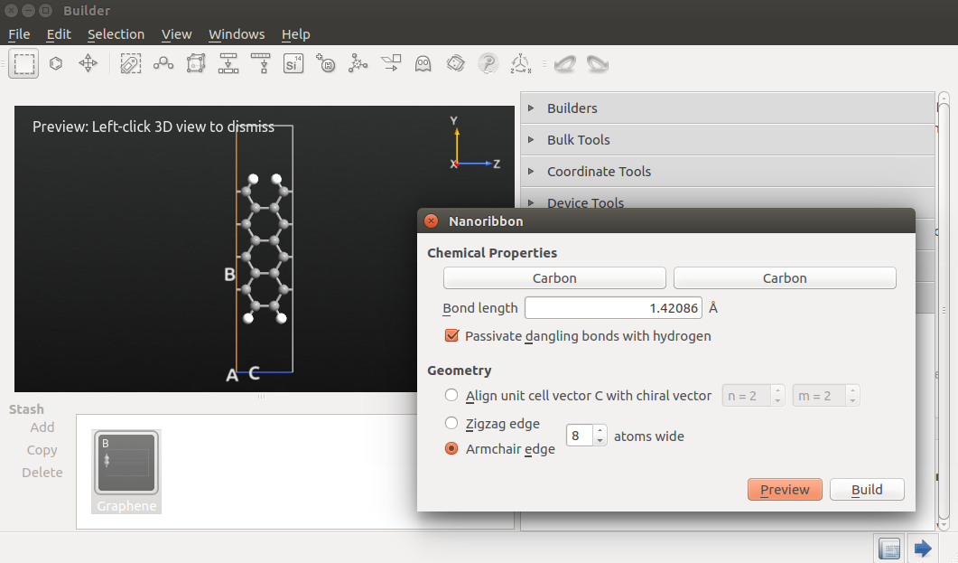
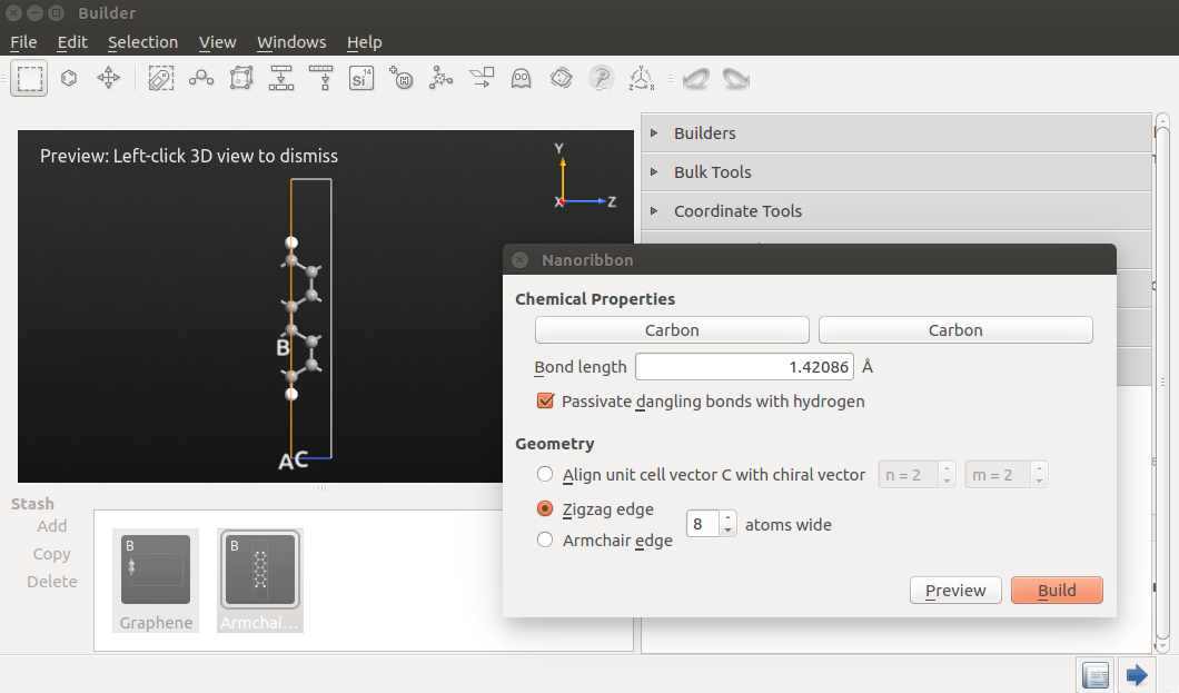
Generating nanoribbons with QuantumATK could not be easier – there is a Builder plugin specifically
designed for this task. Launch the Builder and click . This launches
the Graphene Ribbon tool.
In the widget that opens, you can design many different types of nanoribbons, not just graphene but also B-N, etc. By selecting a linear combination nA+mB of the two unit cell vectors A and B in the graphene plane, ribbons of any chirality can be constructed (the “chirality” label comes from the fact that these structure correspond to an unrolled (n,m) nanotube). For simplicty, you can also directly choose to build armchair or zigzag ribbons, and specify their width (which must be even for zigzag ribbons).
Select an armchair ribbon of width 8 (carbon atoms), and click Build to add it to the Stash.
Send the structure to the Script Generator.
Band structure
Like before we will use the Extended Hückel method for the calculations. Change the default output filename to
armchair.hdf5, and add the following two blocks to the script:
- New Calculator
- Bandstructure
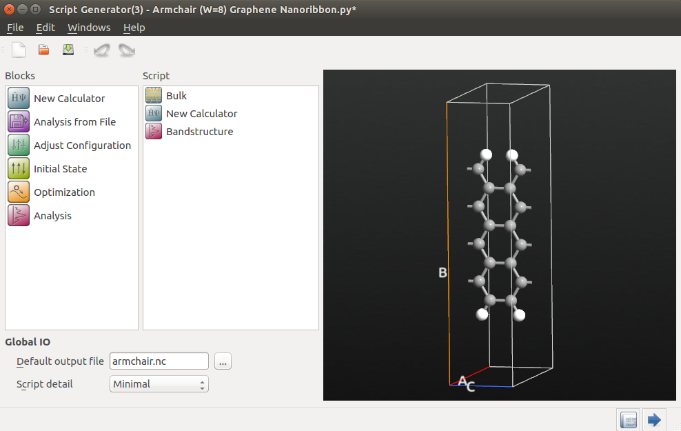
Open the Calculator block to edit it:
Select the “ATK-SE: Extended Hückel” calculator.
Select the “Cerda.Carbon [graphite]” basis set for carbon. The default “Hoffmann” basis set should work well for the hydrogen.
In this case you need only 1 k-point in the directions perpendicular to the direction of the ribbon, since the system is finite in these direction, while the system is periodic in the C direction. A large number of k-points is needed in this direction, since the unit cell is quite short and graphene has a rather peculiar point-like Fermi surface as we saw above; 100 points should be sufficient:
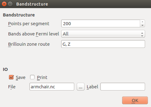
The default suggested route in the Brillouin zone from G=(0,0,0) to Z=(0,0,1/2) for the band structure is indeed the appropriate one, so you just need to increase the number of points to 200 to obtain nicely smooth curves:
Run the calculation using the Job Manager.
Analyzing the results
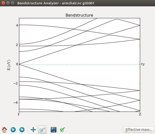
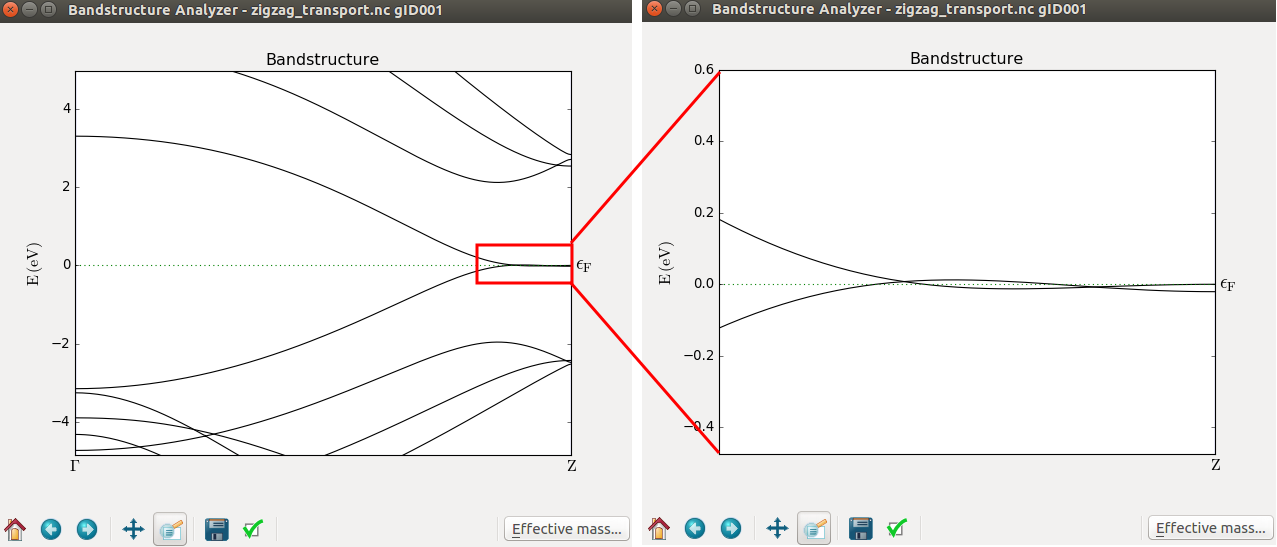
Return to the main QuantumATK window and use the Bandstructure Analyzer to plot the Bandstructure item from the file
armchair.hdf5. The computed band structure is shown in the figure below. By zooming in a bit you should
see a small band gap band gap at the Γ point. The armchair nanoribbon is therefore semiconducting.
As an extension of this exercise, you are recommended to redo the calculations for different types of ribbons (armchair/zigzag) and for different widths. The band gap is strongly dependent on both factors!
In the next section, you will investigate a zigzag ribbon, which is metallic rather than semiconducting.
Transport properties of a zigzag nanoribbon
In this section you will do some transport calculations. One of the most basic transport system that can be made with graphene is a perfect, infinite zigzag nanoribbon. Such ribbons are metallic and display no elastic scattering, i.e. perfect conductivity. In the second part you will investigate what happens when scattering is introduced by distorting the edges of the ribbon.
Pristine ribbon
In a pristine device system there is no scattering from the central region and, as illustrated in the following, you can obtain the transmission spectrum from the properties of the electrode.
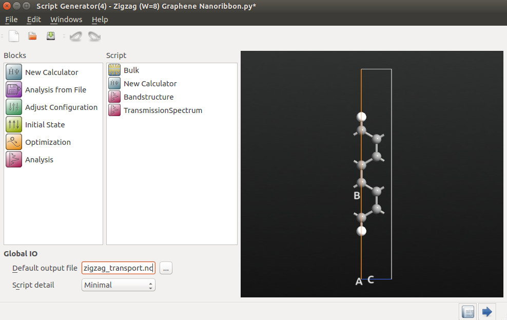
Return to the Builder and open the Nanoribbon widget from . Build a zigzag nanoribbon with a width of 8 carbon atoms.
Transfer the structure to the Script Generator and add the following blocks to the script.
- New Calculator
- Bandstructure
- TransmissionSpectrum
Change the default output file to zigzag_transport.hdf5.
Edit the Calculator settings:
Select the Extended Hückel calculator
Set the k-point sampling to 1x1x100.
Change the Hückel basis set to “Cerda.Carbon [graphite]” for C.
Next, open the the Bandstructure block and set points per segment to 200.
Finally, open the TransmissionSpectrum block and set the energy range from −4 eV to +4 eV.
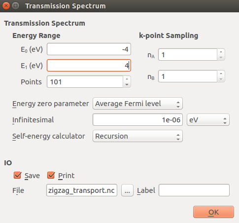
Note
The odd number of energy points ensures that there will be an energy point at the Fermi level.
Run the script using the Job Manager. It should take only a few minutes to finish.
Analyzing the results
Once the calculation finishes, locate the TransmissionSpectrum item on the LabFloor, and open the Transmission Analyzer plugin. As expected for a perfect 1D system, the transmission exhibits a sequence of steps with integer transmission.
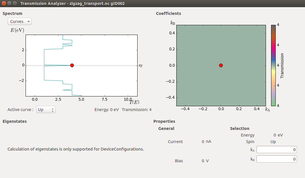
The most prominent feature of the plot is the enhanced transmission around the Fermi level. This is due to a peculiarity in the band structure of the zigzag ribbon (see the band structure below), and interestingly enough, the enhancement is retained even if the ribbon is distorted, at least in the way that will be investigated in the next example.
Creating a distortion in the ribbon
So far you have basically just confirmed that armchair ribbons are semiconducting and zigzag ribbons are metallic (at least as long as electron spin is not considered). It is now time to do something a little bit more interesting. The next system you will study is a distorted ribbon; more specifically you will make a constriction in the perfect zigzag ribbon, and see how this influences the transport properties.
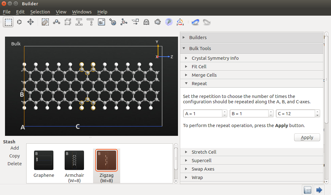
Return to the Builder and open the “Repeat” tool (available from “Bulk Tools” in the plugin panel).
Set C=12 and click Apply. Then press Ctrl+R to reset the 3D view.

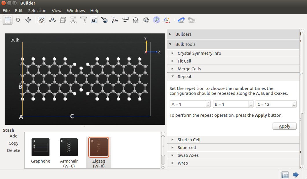
Select the atoms indicated in the figure below by drawing a rectangle with the mouse, while holding down Ctrl.
Delete the atoms by pressing the Delete key. The dangling bonds that have now been created should be saturated by
adding hydrogen atoms. To do this, click the “Passivate” button on the top toolbar.
Finally, convert the periodic structure to a device geometry by using the tool.
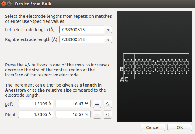
The builder will detect any pattern of periodicity close to the edges of the structure, and suggest these as electrodes. You may see these suggestions in the dropdown combo boxes, as indicated in the figure above.
For the current structure, several periodicity patterns can be found, corresponding to a certain number of repetitions of the zigzag unit cell. The suggested value (7.383 Å), corresponds to 3 repetitions, and this is a suitable length. Thus, no further adjustments are needed. Click OK, to build the device geometry for the distorted zigzag nanoribbon.
Transport properties of the distorted ribbon
In the following you will learn how to perform the calculation of the zero-bias conductance of the distorted ribbon using open boundary conditions, first non-self consistently and then self-consistently.
Note
Calculations at finite bias must always be performed fully self-consistently, since the non-self-consistent model do not produce a correct voltage drop across the device.
Non-self-consistent calculation
Send the device geometry to the Script Generator, and set the default output file name
to zigzag_transport.hdf5 (i.e. the same file name as used for the bulk transmission calculation above,
so that the new calculations are saved in that same file).
Then add the New Calculator and TransmissionSpectrum script blocks.
Set up the Calculator block to use the Extended Hückel (Device) calculator with the “Cerda.Carbon[graphite]” Hückel basis set for carbon. Set also the energy range in the TransmissionSpectrum block to −4 eV to +4 eV.
Run the script using the Job Manager. It takes a minute or so, but while it is running you can
already proceed and prepare the next step.
Self-consistent calculation
You should also perform a self-consistent calculation with open boundary conditions. This requires only a single
change to the Calculator block:
Remove the tick mark from No SCF iteration in the “Iteration Control Parameters” calculator settings.
Send the script to the Job Manager and run the job.
Run the script using the Job Manager. This time the job will take somewhat longer
(around 10 minutes).
Comparing the transmission spectra
Let us now compare the computed transmission spectra of the perfect ribbon and the distorted ones. On the LabFloor, select Item Type in the “Group by” menu. Then select all three the transmissionspectrum objects and click the Compare Data plugin.
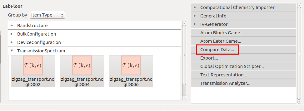
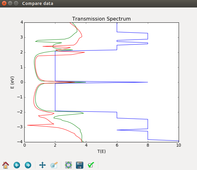
Fig. 84 Comparison of the transmission spectra of a perfect ribbon (blue) and a distorted ribbon calculated non-selfconsistently (green) and selfconsistently (red).
Comparing the results you see that the strong transmission at the Fermi level in the perfect ribbon is also present in the distorted ribbon. Apart from this, the transmission spectra for the distorted GRN are strongly suppressed due to scattering by the distortion.