Slater-Koster tight-binding models in ATK-SE
Version: 2017.0
ATK-SemiEmpirical (ATK-SE) comes preloaded with Slater-Koster parameters for simple systems like Si and GaAs, using a couple of different nearest-neighbor models like sp3s* and sp3d5s*. One very important feature of ATK-SE is, however, that it is possible to manually define custom Slater-Koster parameters, e.g. found in scientific literature, and this will be demonstrated in this tutorial.
The tutorial considers a nearest-neighbor Slater-Koster model for hydrogen-passivated silicon, which can for example be used to simulate H-terminated Si nanowires.

Introduction
There are two primary ingredients in a Slater-Koster (SK) model for electronic structure calculations:
The values of the onsite matrix elements for each element (or atom types) in the model.
The values of the offsite (hopping) matrix elements for each pair of atom types in the model, and how these depend on the distance between the atoms.
These points will be discussed extensively in this tutorial.
Nearest-neighbor model for silicon with placeholder hydrogen atoms
We will use the Boykin-type sp3d5s* model by Zheng et al. [1], which is a commonly used Slater-Koster parametrization for studying Si nanowires. The model extends an earlier parametrization of Si and Ge [2], which in turn builds on the original sp3d5s* models by Jancu et al. [3]. The latter is available as a built-in basis set in QuantumATK (denoted “Bassani”).
Note
The Boykin-type Slater-Koster model implemented in this tutorial will be available as a built-in basis set in QuantumATK as of the 2018 release.
The first step is to define the SK model for Si according to Ref. [2], then the hydrogen matrix elements will be added to the model in a second step according to Ref. [1]. These are used to remove spurious electronic states due to dangling Si surface bonds, so they basically constitute a numerical trick.
Onsite matrix element
First, consider the onsite matrix element. Here you need to specify the angular momenta, number of valence electrons, ionization potentials and spin-orbit split of the basis orbitals. The onsite Hartree shift and spin split are taken from built-in databases in QuantumATK.
The ionization potentials and spin-orbit split can be taken directly from Ref. [2]. There are four types of valence orbitals (3s, 3p, 3d, and an excited s-type orbital, commonly denoted s* in literature). The onsite Hartree shifts can be extracted from a built-in database; for the unoccupied orbitals 3d and s* will use the values from the occupied valence orbitals. The spin splits are also obtained from a built-in database.
The onsite matrix elements for each element in the basis set
are specified as instances of the SlaterKosterOnsiteParameters ATKPython class.
For the present silicon SK model, we use the variable onsite for an
instance of this class:
# Define ionization potentials
Es    = -2.15168*eV
Ep    =  4.22925*eV
Ed    = 13.78950*eV
Es1   = 19.11650*eV

# Define spin-orbit split
split =  0.01989*eV

onsite = SlaterKosterOnsiteParameters(
            element                     = Silicon,
            angular_momenta             = [0,1,2,0],
            number_of_valence_electrons = 4,
            filling_method              = SphericalSymmetric,
            ionization_potential        = [Es,Ep,Ed,Es1],
            onsite_hartree_shift=ATK_U(PeriodicTable.Silicon, ["3p"], 'ncp')[0],
            onsite_spin_split=ATK_W(PeriodicTable.Silicon, [ "3p", "3p", "3p", "3s" ]),
            onsite_spin_orbit_split=[0.0,2*split, 0.0, 0.0]*eV,
           )
Note that the element for which these onsite parameters apply to is
a required argument.
Tip
Occupations: What actually happens when specifying
number_of_valence_electrons = 4 is that the four electrons are
equally distributed among all the 10 available orbitals.
This gives the following electron occupations of the Slater-Koster orbitals:
- 3s:
(4/10) electrons * 1 s-type orbital = 0.4
- 3p:
(4/10) electrons * 3 p-type orbitals = 1.2
- 3d:
(4/10) electrons * 5 d-type orbitals = 2.0
- s*:
(4/10) electrons * 1 s-type orbital = 0.4
These occupations could also have been directly specified in the
SlaterKosterOnsiteParameters instead of specifying the
total number of electrons:
onsite = SlaterKosterOnsit+eParameters(
            element                       = Silicon,
            angular_momenta               = [0,1,2,0],
            # number_of_valence_electrons = 4,
            occupations                   = [0.4, 1.2, 2.0, 0.4],
Offsite matrix elements
A Slater-Koster model is in general not based on the concept of neighbors – the offsite (hopping) matrix elements are instead defined in a range of distances around each atom, possibly using a scaling function to specify the distance-dependence of the Hamiltonian matrix element. A cut-off distance should also be specified, above which atoms do not interact (the matrix element is set to zero beyond this distance).
The hopping matrix elements are therefore tabulated in an interval around the silicon nearest-neighbor distance, using values from Ref. [2]:
from math import sqrt

# --------------------------------------------------#
#                     Silicon                       #
#---------------------------------------------------#

# a is the cubic lattice constant
a = 5.431*Ang

# Nearest neighbor distance
d_n1 = sqrt(3.0)/4.0*a
# Second-nearest neighbor distance
d_n2 = sqrt(2.0)/2.0*a

# Setup list of distances
epsilon = numpy.linspace(-0.20, 0.20, 41)
distances = [ d_n1*(1.0+x) for x in epsilon ] + [ 0.5*(d_n1+d_n2) ]

# Setup hopping elements
si_si_sss   = [ -1.95933*eV for x in epsilon ]
si_si_s1s1s = [ -4.24135*eV for x in epsilon ]
si_si_ss1s  = [ -1.52230*eV for x in epsilon ]
si_si_sps   = [  3.02562*eV for x in epsilon ]
si_si_s1ps  = [  3.15565*eV for x in epsilon ]
si_si_sds   = [ -2.28485*eV for x in epsilon ]
si_si_s1ds  = [ -0.80993*eV for x in epsilon ]
si_si_pps   = [  4.10364*eV for x in epsilon ]
si_si_ppp   = [ -1.51801*eV for x in epsilon ]
si_si_pds   = [ -1.35554*eV for x in epsilon ]
si_si_pdp   = [  2.38479*eV for x in epsilon ]
si_si_dds   = [ -1.68136*eV for x in epsilon ]
si_si_ddp   = [  2.58880*eV for x in epsilon ]
si_si_ddd   = [ -1.81400*eV for x in epsilon ]
Note that the cut-off distance is taken at the midpoint between the first and second nearest neighbors (the separate element added to the list), where the corresponding matrix element is set to zero.
Important
The hopping matrix elements defined above are only valid for silicon with a lattice constant of 5.431 Å.
However, the scaling function for the matrix elements could also be fitted to allow calculations for more irregular structures. In that approach, it is commonly assumed that the matrix elements \(ijk(d)\) follow a power law,
where \(d_0\) is the ideal neighbor distance. Harrison [4] originally used a general exponent of \(n_{ijk}=2\) for all matrix elements \(ijk\), but later work, e.g. [3] and [5], extends this to fit an individual exponent for each matrix element.
Defining the full Slater-Koster table
In QuantumATK, the Slater-Koster basis set should be implemented as an instance of the
SlaterKosterTable ATKPython class.
As explained in detail in the ATK Manual,
the onsite and offsite matrix elements in the SlaterKosterTable
are defined using special keyword arguments.
Onsite parameters
The onsite matrix element for Si is simply passed to the
SlaterKosterTable using the label silicon:
# Create Slater-Koster table
basis_set = SlaterKosterTable(silicon     = onsite,
Offsite parameters
All the offsite matrix elements defined above are given as individual keyword arguments
when setting up the SlaterKosterTable.
As explained in the ATK Manual,
these arguments must be on the form element1_element2_XYZ=list,
where X and Y are the labels of the orbitals on the first and second elements
(both can be s, p, d, or f),
while Z is the type of interaction
(s, p, or d for \(\sigma\), \(\pi\), or \(\delta\), respectively).
Thus, for example, the \(\mathrm{sd} \pi\) offsite matrix element
between carbon and silicon in some hypothetical SK model
would be set with the keyword si_c_sdp.
In the present case of pure silicon, the full Slater-Koster table definition, including both onsite and offsite parameters, becomes as follows:
# Create Slater-Koster table
basis_set = SlaterKosterTable(silicon     = onsite,
                              si_si_sss   = zip(distances,si_si_sss),
                              si_si_s1s1s = zip(distances,si_si_s1s1s),
                              si_si_ss1s  = zip(distances,si_si_ss1s),
                              si_si_sps   = zip(distances,si_si_sps),
                              si_si_s1ps  = zip(distances,si_si_s1ps),
                              si_si_sds   = zip(distances,si_si_sds),
                              si_si_s1ds  = zip(distances,si_si_s1ds),
                              si_si_pps   = zip(distances,si_si_pps),
                              si_si_ppp   = zip(distances,si_si_ppp),
                              si_si_pds   = zip(distances,si_si_pds),
                              si_si_pdp   = zip(distances,si_si_pdp),
                              si_si_dds   = zip(distances,si_si_dds),
                              si_si_ddp   = zip(distances,si_si_ddp),
                              si_si_ddd   = zip(distances,si_si_ddd),
                             )
Note
Some additional remarks:
The order of the element labels
XandYmatters, if there is more than one element in the model. The orbitaliis associated with the elementXorbital, andjwithY.The element labels are not case-sensitive and may be abbreviated. Thus,
Si,si, orSiliconare all accepted for silicon.
Tip
This present SK basis set contains two s-type orbitals (3s and s*). To distinguish orbitals of the same angular momentum, there are two things to keep in mind:
For the onsite elements, the identification is made by the ordering of the ionization potentials vs. the occupations and angular momenta, etc.
For the offsite elements, a running index is added, so the first s-orbital is “s0”, the second one “s1”, etc. The “0” for the first orbital can be omitted to reduce the notation, so as you see above, the \(\mathrm{s}*\mathrm{p}\sigma\) matrix element will be defined by the keyword
si_si_s1ps, etc.
Full script
The full script defining the silicon Slater-Koster basis set combines all of the script snippets shown above:
from QuantumATK import *

'''
Generate a Slater-Koster basis set for silicon based on
T. B. Boykin et al., PRB 69, 115201 (2004)
http://dx.doi.org/10.1103/PhysRevB.69.115201
'''

from math import sqrt

# --------------------------------------------------#
#                     Silicon                       #
#---------------------------------------------------#

# a is the cubic lattice constant
a = 5.431*Ang

# Nearest neighbor distance
d_n1 = sqrt(3.0)/4.0*a
# Second-nearest neighbor distance
d_n2 = sqrt(2.0)/2.0*a

# Setup list of distances
epsilon = numpy.linspace(-0.20, 0.20, 41)
distances = [ d_n1*(1.0+x) for x in epsilon ] + [ 0.5*(d_n1+d_n2) ]

# Setup hopping elements
si_si_sss   = [ -1.95933*eV for x in epsilon ]
si_si_s1s1s = [ -4.24135*eV for x in epsilon ]
si_si_ss1s  = [ -1.52230*eV for x in epsilon ]
si_si_sps   = [  3.02562*eV for x in epsilon ]
si_si_s1ps  = [  3.15565*eV for x in epsilon ]
si_si_sds   = [ -2.28485*eV for x in epsilon ]
si_si_s1ds  = [ -0.80993*eV for x in epsilon ]
si_si_pps   = [  4.10364*eV for x in epsilon ]
si_si_ppp   = [ -1.51801*eV for x in epsilon ]
si_si_pds   = [ -1.35554*eV for x in epsilon ]
si_si_pdp   = [  2.38479*eV for x in epsilon ]
si_si_dds   = [ -1.68136*eV for x in epsilon ]
si_si_ddp   = [  2.58880*eV for x in epsilon ]
si_si_ddd   = [ -1.81400*eV for x in epsilon ]

# Define ionization potentials
Es    = -2.15168*eV
Ep    =  4.22925*eV
Ed    = 13.78950*eV
Es1   = 19.11650*eV

# Define spin-orbit split
split =  0.01989*eV

onsite = SlaterKosterOnsiteParameters(
            element                     = Silicon,
            angular_momenta             = [0,1,2,0],
            number_of_valence_electrons = 4,
            filling_method              = SphericalSymmetric,
            ionization_potential        = [Es,Ep,Ed,Es1],
            onsite_hartree_shift=ATK_U(PeriodicTable.Silicon, ["3p"], 'ncp')[0],
            onsite_spin_split=ATK_W(PeriodicTable.Silicon, [ "3p", "3p", "3p", "3s" ]),
            onsite_spin_orbit_split=[0.0,2*split, 0.0, 0.0]*eV,
           )

# Create Slater-Koster table
basis_set = SlaterKosterTable(silicon     = onsite,
                              si_si_sss   = zip(distances,si_si_sss),
                              si_si_s1s1s = zip(distances,si_si_s1s1s),
                              si_si_ss1s  = zip(distances,si_si_ss1s),
                              si_si_sps   = zip(distances,si_si_sps),
                              si_si_s1ps  = zip(distances,si_si_s1ps),
                              si_si_sds   = zip(distances,si_si_sds),
                              si_si_s1ds  = zip(distances,si_si_s1ds),
                              si_si_pps   = zip(distances,si_si_pps),
                              si_si_ppp   = zip(distances,si_si_ppp),
                              si_si_pds   = zip(distances,si_si_pds),
                              si_si_pdp   = zip(distances,si_si_pdp),
                              si_si_dds   = zip(distances,si_si_dds),
                              si_si_ddp   = zip(distances,si_si_ddp),
                              si_si_ddd   = zip(distances,si_si_ddd),
                             )
Silicon band structure
A simple test case for the custom silicon Slater-Koster model is to compute the band structure of silicon:
# -*- coding: utf-8 -*-
# -------------------------------------------------------------
# Silicon
# -------------------------------------------------------------
lattice = FaceCenteredCubic(5.431*Angstrom)
elements = [Silicon, Silicon]
fractional_coordinates = [[ 0.  ,  0.  ,  0.  ],
                          [ 0.25,  0.25,  0.25]]
bulk_configuration = BulkConfiguration(
    bravais_lattice=lattice,
    elements=elements,
    fractional_coordinates=fractional_coordinates
    )
# -------------------------------------------------------------
# Calculator
# -------------------------------------------------------------
from SiBasisSet import basis_set
k_point_sampling = MonkhorstPackGrid(9,9,9,force_timereversal=False)
numerical_accuracy_parameters = NumericalAccuracyParameters(
    k_point_sampling=k_point_sampling,
    density_mesh_cutoff=10.0*Hartree,
    )
calculator = SlaterKosterCalculator(
    basis_set=basis_set,
    numerical_accuracy_parameters=numerical_accuracy_parameters,
    spin_polarization=SpinOrbit,
    )
bulk_configuration.setCalculator(calculator)
nlprint(bulk_configuration)
bulk_configuration.update()
nlsave('si_bs.hdf5', bulk_configuration)

# -------------------------------------------------------------
# Bandstructure
# -------------------------------------------------------------
bandstructure = Bandstructure(
    configuration=bulk_configuration,
    route=[['L', 'G', 'X', 'W', 'K', 'L', 'W', 'X', 'U'],['K', 'G']],
    points_per_segment=50
    )
nlsave('si_bs.hdf5', bandstructure)
Download this script,
as well as the script SiBasisSet.py containing the Si basis set,
and save them in your QuantumATK Project Folder.
Use the  Job Manager to run the script
 si_bs.py,
or run it from a terminal:
atkpython si_bs.py
The job should finish in a few seconds, and produces a very accurate band structure of silicon with an indirect band gap of 1.13 eV.
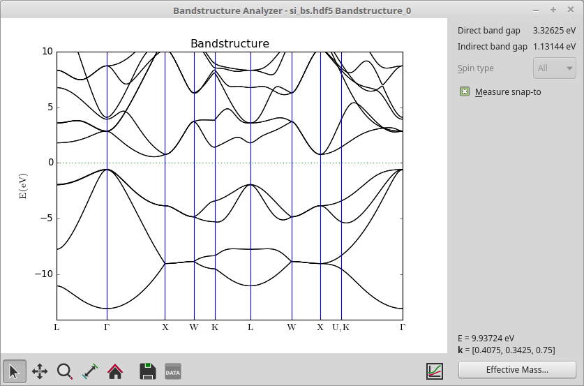
Note
The energy bands in Si are degenerate at the U and K points, and by the special way we construct the band structure route in the script, the band structure plot makes a discontinuous break in the route between these points, i.e. it goes from X to U, then jumps to K and continues to \(\Gamma\).
Adding hydrogen
The goal of this tutorial is to enable modeling of H-terminated Si nanowires, so we need to expand the Slater-Koster table with the parameters for hydrogen from Ref. [1]. As previously discussed, the role of the hydrogen atoms is to eliminate the effects of the unsaturated Si bonds on the surface of the wire, not to represent “real” hydrogen atoms. In an experiment it is of course quite possible that hydrogen atoms, or other atoms, will attach themselves to these dangling bonds, but that is not the point here.
The onsite matrix element for hydrogen is added like this:
# Define ionization potentials
Es_H    =  0.999840*eV

onsite_H = SlaterKosterOnsiteParameters(
                element                 = Hydrogen,
                angular_momenta         = [0],
                occupations             = [1.0],
                ionization_potential    = [Es_H],
                filling_method          = SphericalSymmetric,
                onsite_hartree_shift    = ATK_U(PeriodicTable.Hydrogen, ['1s']),
                onsite_spin_split       = [[0.0]]*eV,
                onsite_spin_orbit_split = [0.0]*eV,
                vacuum_level            = 0.0*Hartree,
Specifying the offsite parameters is done like this:
# reference distances
d_h_n1 = 1.4*Angstrom
d_h_n2 = 2.2*Angstrom

# Setup list of distances
h_distances = [d_h_n1 * (1.0+r) for r in epsilon] + [0.5 * (d_h_n1+d_h_n2)]

# Setup hopping elements
h_si_sss  = [ -3.999720*eV / 1.0 for r in epsilon ]
h_si_ss1s = [ -1.697700*eV / 1.0 for r in epsilon ]
h_si_sps  = [  4.251750*eV / 1.0 for r in epsilon ]
h_si_sds  = [ -2.105520*eV / 1.0 for r in epsilon ]
The onsite and offsite parameters are then simply added to the already prepared
silicon SlaterKosterTable:
from QuantumATK import *

'''
Generate a Slater-Koster basis set for silicon based on
T. B. Boykin et al., PRB 69, 115201 (2004)
http://dx.doi.org/10.1103/PhysRevB.69.115201
'''

from math import sqrt

# --------------------------------------------------#
#                     Silicon                       #
#---------------------------------------------------#

# a is the cubic lattice constant
a = 5.431*Ang

# Nearest neighbor distance
d_n1 = sqrt(3.0)/4.0*a
# Second-nearest neighbor distance
d_n2 = sqrt(2.0)/2.0*a

# Setup list of distances
epsilon = numpy.linspace(-0.20, 0.20, 41)
distances = [ d_n1*(1.0+x) for x in epsilon ] + [ 0.5*(d_n1+d_n2) ]

# Setup hopping elements
si_si_sss   = [ -1.95933*eV for x in epsilon ]
si_si_s1s1s = [ -4.24135*eV for x in epsilon ]
si_si_ss1s  = [ -1.52230*eV for x in epsilon ]
si_si_sps   = [  3.02562*eV for x in epsilon ]
si_si_s1ps  = [  3.15565*eV for x in epsilon ]
si_si_sds   = [ -2.28485*eV for x in epsilon ]
si_si_s1ds  = [ -0.80993*eV for x in epsilon ]
si_si_pps   = [  4.10364*eV for x in epsilon ]
si_si_ppp   = [ -1.51801*eV for x in epsilon ]
si_si_pds   = [ -1.35554*eV for x in epsilon ]
si_si_pdp   = [  2.38479*eV for x in epsilon ]
si_si_dds   = [ -1.68136*eV for x in epsilon ]
si_si_ddp   = [  2.58880*eV for x in epsilon ]
si_si_ddd   = [ -1.81400*eV for x in epsilon ]

# Define ionization potentials
Es    = -2.15168*eV
Ep    =  4.22925*eV
Ed    = 13.78950*eV
Es1   = 19.11650*eV

# Define spin-orbit split
split =  0.01989*eV

onsite = SlaterKosterOnsiteParameters(
            element                     = Silicon,
            angular_momenta             = [0,1,2,0],
            number_of_valence_electrons = 4,
            filling_method              = SphericalSymmetric,
            ionization_potential        = [Es,Ep,Ed,Es1],
            onsite_hartree_shift=ATK_U(PeriodicTable.Silicon, ["3p"], 'ncp')[0],
            onsite_spin_split=ATK_W(PeriodicTable.Silicon, [ "3p", "3p", "3p", "3s" ]),
            onsite_spin_orbit_split=[0.0,2*split, 0.0, 0.0]*eV,
           )

# --------------------------------------------------#
#                     Hydrogen                      #
#---------------------------------------------------#

# reference distances
d_h_n1 = 1.4*Angstrom
d_h_n2 = 2.2*Angstrom

# Setup list of distances
h_distances = [d_h_n1 * (1.0+r) for r in epsilon] + [0.5 * (d_h_n1+d_h_n2)]

# Setup hopping elements
h_si_sss  = [ -3.999720*eV / 1.0 for r in epsilon ]
h_si_ss1s = [ -1.697700*eV / 1.0 for r in epsilon ]
h_si_sps  = [  4.251750*eV / 1.0 for r in epsilon ]
h_si_sds  = [ -2.105520*eV / 1.0 for r in epsilon ]

# Define ionization potentials
Es_H    =  0.999840*eV

onsite_H = SlaterKosterOnsiteParameters(
                element                 = Hydrogen,
                angular_momenta         = [0],
                occupations             = [1.0],
                ionization_potential    = [Es_H],
                filling_method          = SphericalSymmetric,
                onsite_hartree_shift    = ATK_U(PeriodicTable.Hydrogen, ['1s']),
                onsite_spin_split       = [[0.0]]*eV,
                onsite_spin_orbit_split = [0.0]*eV,
                vacuum_level            = 0.0*Hartree,
               )

# Create Slater-Koster table
basis_set = SlaterKosterTable(silicon     = onsite,
                              hydrogen    = onsite_H,
                              si_si_sss   = zip(distances,si_si_sss),
                              si_si_s1s1s = zip(distances,si_si_s1s1s),
                              si_si_ss1s  = zip(distances,si_si_ss1s),
                              si_si_sps   = zip(distances,si_si_sps),
                              si_si_s1ps  = zip(distances,si_si_s1ps),
                              si_si_sds   = zip(distances,si_si_sds),
                              si_si_s1ds  = zip(distances,si_si_s1ds),
                              si_si_pps   = zip(distances,si_si_pps),
                              si_si_ppp   = zip(distances,si_si_ppp),
                              si_si_pds   = zip(distances,si_si_pds),
                              si_si_pdp   = zip(distances,si_si_pdp),
                              si_si_dds   = zip(distances,si_si_dds),
                              si_si_ddp   = zip(distances,si_si_ddp),
                              si_si_ddd   = zip(distances,si_si_ddd),
                              h_si_sss    = zip(h_distances,h_si_sss),
                              h_si_ss1s   = zip(h_distances,h_si_ss1s),
                              h_si_sps    = zip(h_distances,h_si_sps),
                              h_si_sds    = zip(h_distances,h_si_sds),
                             )
Band gaps of passivated silicon nanowires
Due to quantum confinement, the band gap of silicon nanowires usually increase as the wire thickness decreases. You will here demonstrate this using the Si-H Slater-Koster model defined in the sections above.
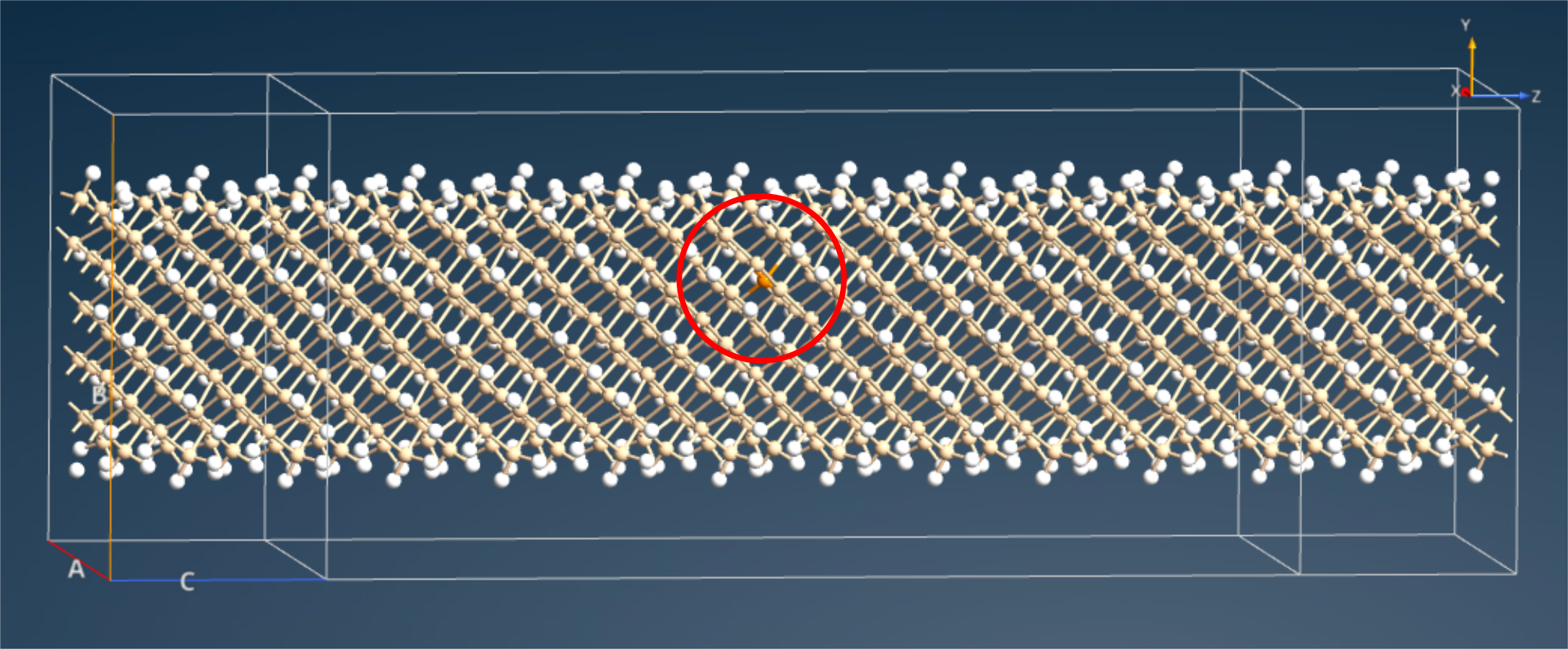
The script wires.py contains 4 silicon nanowire configurations
of different thickness. They are all hydrogen passivated, as exemplified below.
The wires are perdiodic along the Z direction.
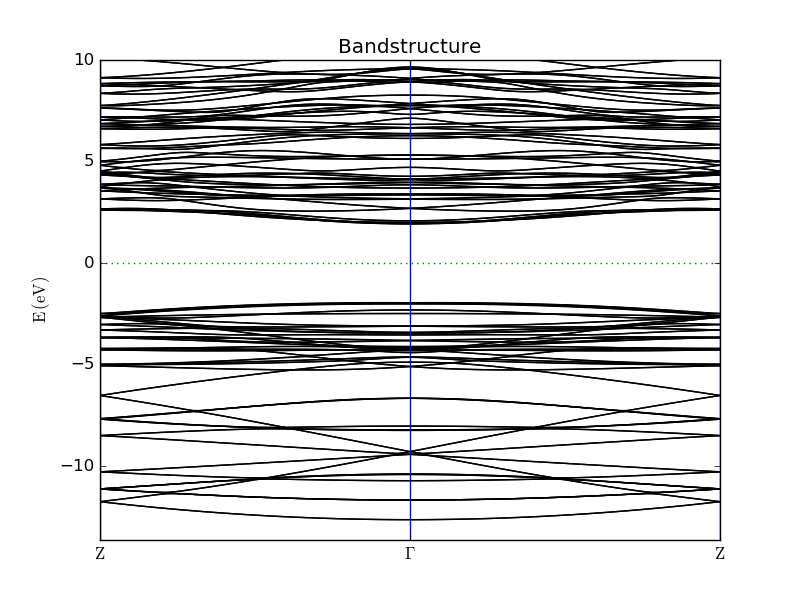
The script nw_bs.py loopes over all 4 nanowires and does a
nonself-consistent Slater-Koster calculation and a bandstructure analysis
for each wire. Results are saved in individual HDF5 data files.
from SiHBasisSet import basis_set
from wires import wire_2x2, wire_3x3, wire_4x4, wire_5x5

for i, wire in zip([2,3,4,5],[wire_2x2,wire_3x3,wire_4x4,wire_5x5]):
    out = 'wire_%ix%i.hdf5' % (i,i)

    # -------------------------------------------------------------
    # Calculator
    # -------------------------------------------------------------
    k_point_sampling = MonkhorstPackGrid(nc=9,force_timereversal=False)
    numerical_accuracy_parameters = NumericalAccuracyParameters(
        k_point_sampling=k_point_sampling,
        density_mesh_cutoff=10.0*Hartree,
        )
    calculator = SlaterKosterCalculator(
        basis_set=basis_set,
        numerical_accuracy_parameters=numerical_accuracy_parameters,
        spin_polarization=SpinOrbit,
        )

    wire.setCalculator(calculator)
    nlprint(wire)
    wire.update()
    nlsave(out, wire)

    # -------------------------------------------------------------
    # Bandstructure
    # -------------------------------------------------------------
    bandstructure = Bandstructure(
        configuration=wire,
        route=['Z', 'G', 'Z'],
        points_per_segment=50
        )
    nlsave(out, bandstructure)
Download both wires.py and nw_bs.py, and save them
in your QuantumATK Project Folder, which should also contain SiHBasisSet.py.
Then execute the script nw_bs.py using the
Job Manager or a terminal – the calculation may take up to 10 minutes to run.
The resulting bandstructure analysis objects should appear on the LabFloor, and you can use the Bandstructure Analyzer to visualize the nanowire band structures. You will find for all 4 wires that the fundamental gap is located at the \(\Gamma\) point, and is significantly larger than the (indirect) band gap of bulk Si.
You can also use the script nw_gaps.py to extract the direct
band gaps and compute the nanowire thicknesses, and to plot the data.
# Read data
gaps = []
lengths = []
for i in [2,3,4,5]:
    out = 'wire_%ix%i.hdf5' % (i,i)
    bandstructure = nlread(out, Bandstructure)[0]
    gap =bandstructure._directBandGap().inUnitsOf(eV)
    gaps.append(gap)
    wire = nlread(out, BulkConfiguration)[0]
    coordinates = wire.cartesianCoordinates().inUnitsOf(nanoMeter)
    indices = numpy.where(numpy.array(wire.symbols())=='Si')[0]
    coords = coordinates[indices][:,0]
    length = max(coords)-min(coords)
    lengths.append(length)

# Plot data
import pylab
pylab.figure(figsize=(8,4))
pylab.plot(lengths, gaps, 'bo-')
pylab.xlabel('Nanowire width (nm)')
pylab.ylabel('Nanowire band gap (eV)')
pylab.tight_layout()
pylab.savefig('nw_gaps.png')
pylab.show()
Running the script produces the plot shown below. The nanowire band gap increase significantly for thicknesses of 1 nm or less, also also found in Ref. [1].
