Elastic scattering, mean free path, mobility: Impurity scattering in a silicon nanowire
Version: 2017.0
In this tutorial you will study elastic scattering by dopant atoms in a silicon nanowire. Based on calculated transmission spectra you will learn how to estimate the scattering mean free path and mobility, taking into account both the effect of doping and the explicit scattering due to the dopant atoms.

Introduction
In this tutorial you will learn how the transmission spectra can be used to estimate the elastic scattering mean free path and the doping dependent mobility.
The main focus of the tutorial is not on the actual calculations of the transmission spectra, but rather on the subsequent analysis. As some of the calculations are rather time-consuming, data-files with the results are provided as downloads, so you can focus on the analysis.
The methods used in the tutorial are based on Ref. [1], where it was shown that the transmission function of a very long silicon nanowires with several structural defects can be accurately reproduced using a statistical average of the transmissions calculated for relatively small nanowires with a single defect.
Theoretical background
At low temperatures, the conductance of a system can be approximated as \(G = G_0 \cdot T(E_F)\), where \(G_0=2e^2/h\) is the conductance quantum and \(T(E_F)\) is the transmission at the Fermi energy. The resistance of the system is \(R=1/G\).
These considerations can be generalized to define an energy dependent and unitless resistance \(R(E)=1/T(E)\), which is just the inverse of the transmission. To get a physical resistance, \(R(E)\) should be multiplied with \(1/G_0\).
For a one-dimensional system without any defects (pristine), the transmission always takes integer values, \(T_0(E)=N(E)\). We shall denote the corresponding resistance \(R_c(E)=1/T_0(E)\) as the contact resistance. If a structural defect (labeled as 1 in the following) is introduced to the system, the transmission will always be lower than the transmission of the pristine system, \(T_1(E)<T_0(E)\). We will now write the resistance of the system with the defect as a sum of two contributions:
which defines the scattering resistance \(R_{1,s}(E)\) of defect 1. If multiple different defects are present – this could be dopant atoms in different positions – we can calculate an average transmission \(\langle T(E) \rangle\). Using the same notation as in the equation above, we will define an average scattering resistance, \(\langle R_s(E) \rangle\), as:
It was shown in Ref. [1] that the length- and energy-dependent resistance through a long wire of length \(L\) containing many, randomly placed defects with an average defect–defect distance \(d\), can be well approximated as:
which may be written as
which defines the energy-dependent scattering mean free path as
Note
Note that we have now introduced the total length of the wire \(L\), which in this formalism is an arbitrary parameter.
The corresponding transmission through the long wire is \(T(L,E) = 1/R(L,E)\). This means that the conductance of a wire with length \(L\) can be estimated as
which generalizes the previous relation \(G=G_0 T(E_F)\) to finite temperatures. The function \(f(E,E_F)\) is the Fermi-Dirac distribution function for electrons in the left and right electrodes with average Fermi level \(E_F\).
The conductivity \(\sigma\) of the system is given by
and we can now estimate the mobility \(\mu\) as
where \(e\) is the elementary charge and \(n\) is the charge density. The Fermi level at a given doping density will be estimated from band structure calculations with compensation charge doping.
Summary of required calculations
In summary, the calculations we need in order to calculate a mean free path are:
Transmission spectrum, \(T_0(E)\), of the pristine (defect free) nanowire.
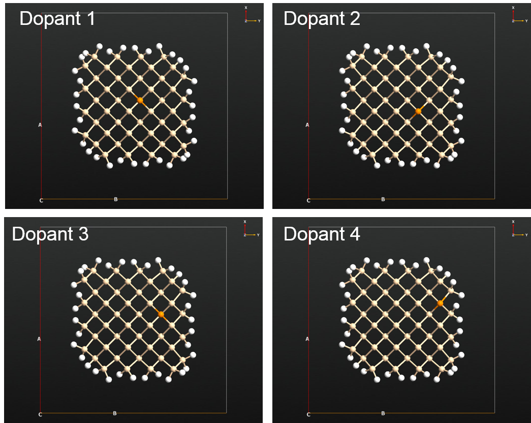
A transmission spectrum for each defect – in this case for the same element in four different dopant positions. From these calculations we get the average transmission \(\langle T(E) \rangle\).
In order to calculate the mobility at a given doping density, we further need:
A bandstructure calculation (also using the nanowire unit cell) with compensation charge doping, in order to calculate the Fermi level for the desired doping density.
Defected silicon nanowires
Two different types of nanowires will be considered:
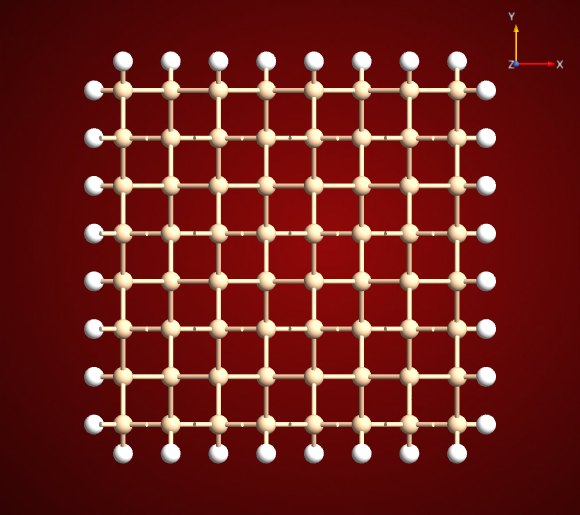
The pristine device is constructed from pure, defect-free, relaxed silicon, passivated with hydrogen at the surface;
The defected devices are generated by substituting one Si atom with P (in 4 different positions) and are relaxed as bulk.
More information on how to build the structures can be found at the end of the tutorial, in the Appendix: Building the nanowires.
Computational method: The calculations are performed with DFT and NEGF, using a GGA xc-functional and the FHI-SZP basis sets. We use 1x1x51 k-points for the NEGF calculations.
Transmission spectra
The calculated transmission spectra are available via download. They have been calculated using 201 points in an energy range between \(E-E_\mathrm{F} = 0.5 eV\) and \(E-E_\mathrm{F} = 2.0 eV\).
For the pristine nanowire, the transmission is calculated for the infinite bulk.
sinw_pristine_trans.hdf5For the defected nanowires, we have used a two-probe device configuration.
sinw_P_dopant_trans_1234.hdf5
Elastic scattering mean free path
In this section, we will analyze how the presence of an impurity atom impacts the transmission through the nanowire, and we will also estimate the mean free path for the conduction electrons. The script T_and_mfp.py calculates and plots the transmission and the mean free path using the theory described in the theoretical background.
The script does the following:
Aligns the conduction band minima, to give the two datasets a common energy reference.
Calculates the scattering resistance \(R_{s}(E)\) from the average transmission and the contact resistance \(R_{c}(E)\) from the pristine transmission.
Saves the data to a file, for re-use later.
Calculates the mean free path from \(R_{c}(E)\) and \(R_{s}(E)\) and the average distance between dopant atoms.
Plots of transmissions and mean free path as functions of energy.
Run the script as atkpython T_and_mfp.py or with the Job Manager, in the directory where you have saved the files with the transmission spectra, and the following figure should appear:
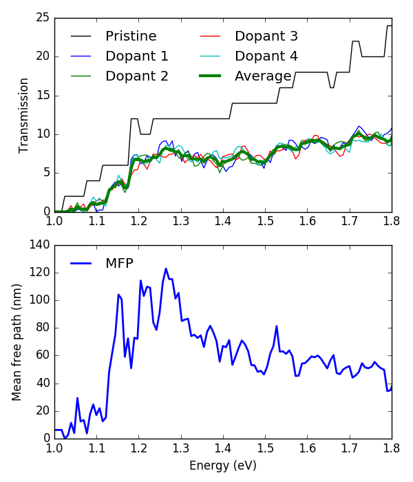
The first plot compares the transmission function for the pristine and the defected nanowires. It can be seen that the transmission of the defected nanowires is similar and always lower than that of the pristine nanowire. The second plot shows the mean free path as a function of energy.
Note how, close to the conduction band edge at energies between 1.0 eV and 1.2 eV, the electrons are strongly scattered by the dopant impurity, and the associated transmission functions are very low. This is reflected in a short mean free path. At higher energies E > 1.2 eV, there is less scattering and both the transmission and mean free path are larger.
Fermi levels in doped nanowires
The next task is to estimate the impurity limited mobility as a function of doping density. In order to do this, you need to know the position of the Fermi level relative to the conduction band edge. This can be achieved by calculating the band structure for silicon nanowires which are uniformly doped. This can be done in QuantumATK using atomic compensation charges. You can learn about doping in QuantumATK in the technical note here: Doping methods available in QuantumATK and in the tutorial here: Silicon p-n junction. The bandstructure calculations use 1x1x9 k-points and the \(\mathrm{\Gamma} \to \mathrm{Z}\) route. You can download the data files here: doped-bandstructures.zip.
After unzipping the files you can compare the bandstructures in QuantumATK using the Bandstructure Analyzer:
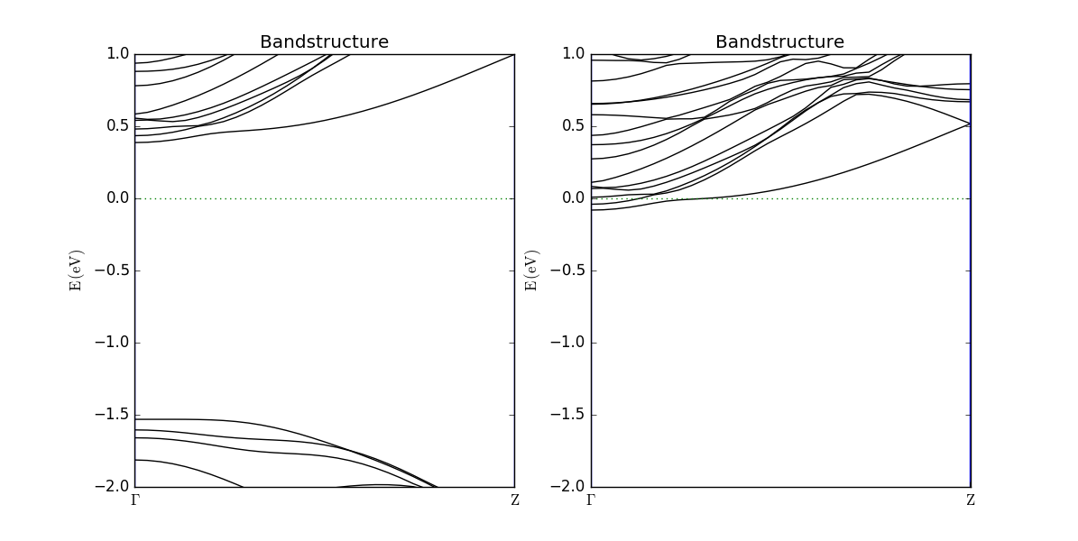
Note that in this case, both bandstructures are referenced to the Fermi level, and it is therefore also easiest to align them here. This means that we need to look at the positions of the bands to study the shift in the Fermi level. We see that the conduction band has shifted about 0.5 eV down when going from a doping level of \(10^{14}\ \mathrm{cm}^{-3}\) to \(10^{21}\ \mathrm{cm}^{-3}\), which is more properly described as the Fermi level shifting up with increasing doping.
Doping dependent mobility
You now have the ingredients needed to estimate the mobility as function of doping concentration. The python script below loads the calculated data and calculate the conductivity as well as mobility for a \(1\ \mu \mathrm{m}\) long Silicon nanowire. By calculating the mobility in this way, as also described in the theoretical background, the following assumptions are made:
Each dopant atom is fully ionized and contributes with one electron to the conduction band charge density.
The transmission of the long wire can be estimated from the single-dopant transmissions.
Warning
Note that the mobility defined in this way is very much an estimate of the mobility of electrons for the pristine wire, as we do not include any explicit scattering mechanisms. It is not directly comparable with the, for the pristine wire more appropriate, mobility that is calculated by f.ex. the Mobility class.
Notice that although the transmission calculations with the dopant atoms to some extend include the doping effect - i.e. that the P atom becomes partly ionized - this effect is not included in the position of the Fermi level, which is determined by the electrodes, which are un-doped in this calculation. The bandstructure calculations with the compensation charge doping are thus needed to consider this effect. You can download the script for these calculations here: mobility.py. The script does the following:
Calculates the conductances and mobilities starting from the transmission;
The conductances and mobilities are plotted as a function of doping level, both with and without taking scattering processes due to dopant atoms into account.
Run the script as atkpython mobility.py, and the following figure should appear:
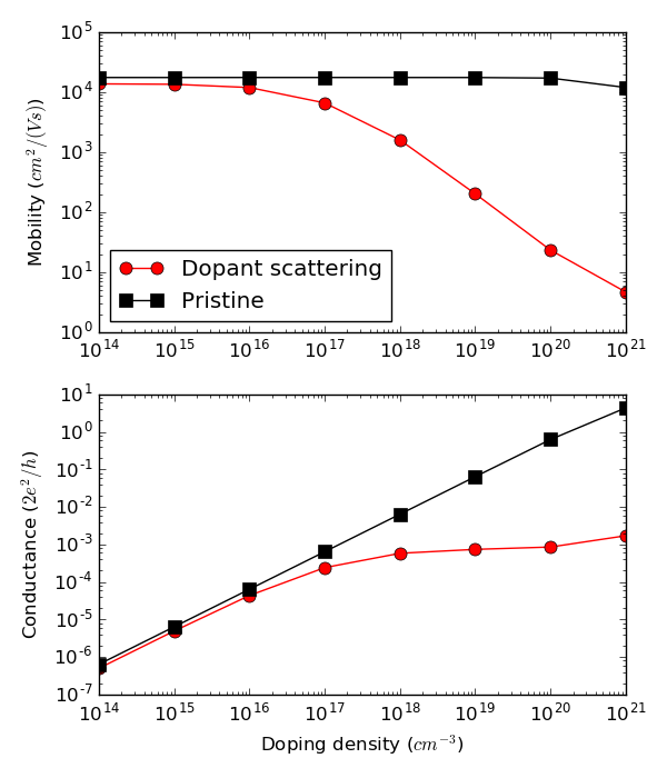
Both the mobility and the conductance are calculated and plotted for two cases:
Including dopant scattering in the transmission calculation of the long wire (red circles).
For a pristine, but uniformly doped, wire transmission (black squares).
When the dopant scattering is included, two factors affect the conductance:
As for the pristine wire case, the Fermi level moved closer to the conduction band for increased doping density. This effect increases the conductance.
Due to the scattering by the dopant impurities, the energy resolved resistance increases linearly with length according to the equations shown in the theory. This effect will decrease the conductance.
From the conductance plot (bottom), one can observe that the two effects approximately cancel out for doping densities \(n > 10^{18}\ \mathrm{cm}^{-3}\), where the conductance is more or less constant. Since the conductance is constant, the mobility will decrease as \(\mu \propto 1/n\) for \(n > 10^{18}\ \mathrm{cm}^{-3}\).
For doping levels \(n < 10^{18}\ \mathrm{cm}^{-3}\), the average dopant-dopant distance becomes larger than the wire length of \(1\ \mu \mathrm{m}\) and there will on average be no dopants in the wire, which is the reason why the doped wire curves approach the pristine wire curves. If we had chosen a longer wire, this onset would happen at lower doping concentrations, as it is related to the ratio \(L/L_\mathrm{mfp}(E)\).
Summary and discussion
As mentioned previously, the focus of this tutorial was not so much on how to calculate very accurate and detailed transmission spectra, but rather on how to extract information from them. In the present case of phosphorus dopants in a silicon nanowire we note the following points:
The actual transmission functions and mobilities will depend on the diameter and orientation of the wire.
The transmission might also depend on the basis set, and differ from the one presented here, if e.g. a larger basis set (like DoubleZetaPolarized) is used.
One should also be aware that the analysis presented in this tutorial is not intended to be very quantitative. It rather provides a relatively straightforward approach to estimate the order of magnitude of the elastic scattering by defects. Recall that the actual system considered would be a \(1\ \mu \mathrm{m}\) long nanowire (this would include more than 150,000 atoms) with randomly placed dopants.
Finally, one should notice that the methods presented in this tutorial are applicable to other kinds of structural disorder such as surface defects [2], or surface roughness scattering [3], and can be applied to both electron and phonon transmission spectra [2], [3].
Appendix: Building the nanowires
Detailed instructions for building a Si nanowire can be found in this tutorial: Silicon nanowire field-effect transistor. However, you may also use the Nanowire plugin in the Builder. In this case, we have used a nanowire bounded by (111) and (100) facets and a radius of 7.0 Å.