DFT-1/2 and DFT-PPS density functional methods for electronic structure calculations
Version: R-2020.09
QuantumATK offers two novel density functional corrections for computing the electronic structure of semiconductors and insulators: the DFT-1/2 and pseudopotential projector shift (DFT-PPS) methods. This tutorial gives an introduction to these methods.
DFT-1/2 is often also denoted LDA-1/2 or GGA-1/2, and is a semi-empirical approach to correcting the self-interaction error in local and semi-local exchange-correlation density functionals for extended systems, similar in spirit to the DFT+U method. As such, it can be viewed as an alternative to the TB09-Meta-GGA method with broadly the same aims; to improve the description of conduction-band energy levels and band gaps. Just like with TB09-MGGA, the DFT-1/2 method is not suitable for calculations that rely on total energy and forces, e.g., geometry optimization or molecular dynamics.
PPS is an abbreviation for pseudopotential projector shift. This method introduces empirical shifts of the nonlocal projectors in the SG15 pseudopotentials, in spirit of the empirical pseudopotentials proposed by Zunger and co-workers in [1]. The projector shifts have been adjusted to reproduce technologically important properties of semiconductors such as the fundamental band gap and lattice constant. The PPS method currently works out-of-the-box for the elements silicon and germanium, but may be used for other elements also by manually specifying the appropriate projector shifts (these must somehow first be determined). Importantly, the PPS method does work for geometry optimization of semiconductor material structures.

DFT-1/2 methods
The DFT-1/2 method attempts to correct the DFT self-interaction error by defining an atomic self-energy potential that cancels the electron-hole self-interaction energy. This potential is calculated for atomic sites in the system, and is defined as the difference between the potential of the neutral atom and that of a charged ion resulting from the removal of a fraction of its charge, between 0 and 1 electrons. The total self-energy potential is the sum of these atomic potentials. The addition of the DFT-1/2 self-energy potential to the DFT Hamiltonian has been found to greatly improve band gaps for a wide range of semiconducting and insulating systems [2]. For more information, see the QuantumATK Manual entry on the DFT-1/2 method.
Important
The method is not entirely free of empirical parameters. For eaxmple, a cutoff radius is employed. Following Refs. [3] and [2] it is chosen such as to maximize the band gap.
Note also that not all elements in the system necessarily require the DFT-1/2 correction; it is generally advisable only to add this to the anionic species, and leave the cationic species as normal.
Default DFT-1/2 parameters are available in QuantumATK; these have been optimized against a wide range of materials, and should improve upon the standard LDA or GGA band gap in most cases.
InP bandstructure using PBE-1/2
Create a new QuantumATK project (preferably in a new folder),
and open the  Builder.
Then click
and locate the InP crystal in the Database.
Builder.
Then click
and locate the InP crystal in the Database.

Add the InP cystal to the Builder Stash, and send the configuration
to the  Script Generator.
Then add the following script blocks:
Script Generator.
Then add the following script blocks:
 New Calculator
 Bandstructure
and open the calculator widget to adjust the calculator parameters.
Select a 9x9x9 k-point grid, and navigate to the Basis set/exchange correlation tab. Note that the default exchange-correlation method is “GGA” (PBE). Enable the DFT-1/2 correction by ticking the checkbox indicated below.

Close the calculator widget and save the script as InP.py.
If you open the script using the  Editor,
you will see that the exchange-correlation method is
Editor,
you will see that the exchange-correlation method is GAHalf.PBE:
#----------------------------------------
# Exchange-Correlation
#----------------------------------------
exchange_correlation = GGAHalf.PBE
that is, GGA-1/2 using the PBE functional, which might also be denoted PBE-1/2.
You may download the script here if needed: InP.py
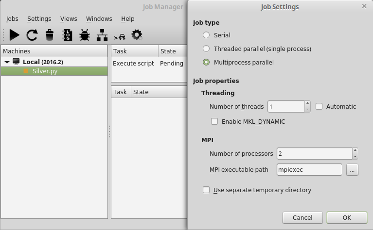
Run the script using either the  Job Manager:
or from a terminal:
$ atkpython InP.py > InP.log
The calculation will be very fast. Once done, use the Bandstructure Analyzer to plot the resulting band structure. You will correctly find that InP is a direct-gap semiconductor with a band band gap of 1.46 eV, which is close to the experimental gap of 1.34 eV from Ref. [4].

Tip
You may want to zoom in on the bands around the Fermi level for a better view. There are two ways to do this:
use the Zoom Tool (third icon from the left);
or click the y-axis label to select it, then right-click and select Edit item in order to open the Axis Properties widget, where you can adjust the limits of the y-axis.

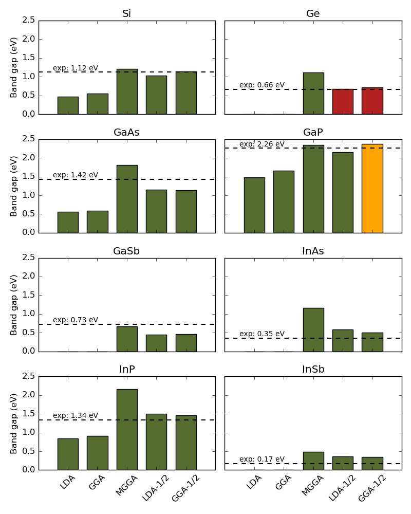
III-V type semiconductor band gaps
The plots below show how the DFT-1/2 methods (LDA-1/2 and GGA-1/2) compare to LDA, GGA, and TB09-MGGA standard band gap calculations using default pseudopotentials and basis sets. A 9x9x9 k-point grid was used in all calculations, and experimental band gaps were adapted from Ref. [4].
It is quite clear that the DFT-1/2 correction improves on standard LDA and GGA band gaps, which are usually too small or non-existing (no bar). TB09-MGGA calculations with self-consistently determined c-parameter also improves band gaps in general.
The red bars for Ge using LDA-1/2 and GGA-1/2 indicate that a direct band gap is wrongly predicted (\(\Gamma\)–\(\Gamma\) instead of \(\Gamma\)–L as in experiments). The orange bar for GaP using GGA-1/2 indicates that the gap is correctly predicted to be indirect, but that the band energy in the L-valley is wrongly predicted to be a little lower than in the X-valley.
Manually specifying DFT-1/2 parameters
It is of course possible to manually specify the DFT-1/2 parameters
instead of using the default ones.
This is done by creating an instance of the DFTHalfParameters
class, which is then given as an argument to the basis set.
For example, let’s consider the case of GaAs. The following script manually sets up
the As DFT-1/2 parameters identical to the default ones,
and leaves the DFT-1/2 correction disabled for Ga, which is also default
behavior. Note the dft_half_parameters argument to the basis set:
#----------------------------------------
# Basis Set
#----------------------------------------
# LDA-1/2 parameters for As
dft_half_parameters = DFTHalfParameters(
    element=Arsenic,
    fractional_charge=[0.3, 0.0],
    cutoff_radius=4.0*Bohr,
    )
# No LDA-1/2 parameters are needed for Ga (Disabled)
basis_set = [
    LDABasis.Arsenic_DoubleZetaPolarized(
        dft_half_parameters=dft_half_parameters),
    LDABasis.Gallium_DoubleZetaPolarized(
        dft_half_parameters=Disabled),
    ]
For more information, see the sections Input format for DFT-1/2 and DFT-1/2 default parameters in the QuantumATK Manual.
Warning
Choosing the appropriate DFT-1/2 parameters may be a very delicate matter, and great care has been taken in determining the default parameters. If you choose to use non-default DFT-1/2 parameters, the quality of those parameters is entirely your own responsibility as a user!
QuantumATK does not offer support for determining custom DFT-1/2 parameters; we recommend in general that users stick to the default ones.
DFT-PPS method
As already mentioned, the DFT-PPS method applies shifts to the nonlocal projectors in the SG15 pseudopotentials. The nonlocal part of the pseudopotential, \(\hat{V}_\text{nl}\), is modified according to
where the sum is over all projectors \(p_{l}\), and \(\alpha_{l}\) is an empirical parameter that depends on the orbital angular momentum quantum number \(l\). Note that this approach does not increase the computational cost of DFT calculations!
The required projector shift parameters have been optimized for silicon and germanium and for use with the PBE density functional and SG15 pseudopotentials only. These are implemented as separate basis sets:
BasisGGASG15.Silicon_LowProjectorShift
BasisGGASG15.Silicon_MediumProjectorShift
BasisGGASG15.Silicon_HighProjectorShift
BasisGGASG15.Silicon_UltraProjectorShift

BasisGGASG15.Germanium_MediumProjectorShift
BasisGGASG15.Germanium_HighProjectorShift
BasisGGASG15.Germanium_UltraProjectorShift
For each element, the same set of optimized projector shifts are applied in
all SG15 basis sets. The script projector_shifts.py prints the built-in DFT-PPS parameters
for Si and Ge:
Si
s-shift: +21.33 eV
p-shift: -1.43 eV
d-shift: +0.00 eV
Ge
s-shift: +14.55 eV
p-shift: +0.20 eV
d-shift: -2.17 eV
Note that the d-shift for Si is 0.0 eV since silicon has no d-electrons.
Si, SiGe, and Ge band gaps and lattice constants
The DFT-PPS method is enabled in the Script Generator
by selecting one of the ProjectorShift basis sets for Si or Ge,
as indicated below. No other calculator settings need to be changed in order
to switch from ordinary PBE to DFT-PPS.

One very convenient aspect of the DFT-PPS method is that it allows for geometry optimization (forces and stress minimization) just like ordinary GGA calculations do – in fact, the DFT-PPS parameters may often be chosen such as to give highly accurate semiconductor lattice constants while also producing accurate band gaps.
In the following, you will consider bulk Si and Ge, and a simple 50/50
SiGe alloy. These 3 bulk configurations are defined in the script bulks.py.
The script pbe.py runs geometry optimization and band structure analysis
for all 3 configurations,
while the script pps.py does the same using the DFT-PPS method.
The latter script looks like shown below. Note the lines from 2 to 31 in that particular script, where the bulk configurations are imported from the external script, and a Python loop over these configurations and basis sets is set up. Also, the DFT-PPS shifts are here manually specified.
 1# -*- coding: utf-8 -*-
 2from bulks import si, ge, sige
 3setVerbosity(MinimalLog)
 4
 5configurations = [si,ge,sige]
 6labels         = ['Si','Ge','SiGe']
 7
 8# Basis set for Silicon
 9SiliconBasis_projector_shift = PseudoPotentialProjectorShift(
10    s_orbital_shift=21.33*eV,
11    p_orbital_shift=-1.43*eV,
12    d_orbital_shift=0.0*eV,
13    f_orbital_shift=0.0*eV,
14    g_orbital_shift=0.0*eV
15    )
16SiliconBasis = BasisGGASG15.Silicon_Medium(projector_shift=SiliconBasis_projector_shift)
17
18# Basis set for Germanium
19GermaniumBasis_projector_shift = PseudoPotentialProjectorShift(
20    s_orbital_shift=14.55*eV,
21    p_orbital_shift=0.20*eV,
22    d_orbital_shift=-2.17*eV,
23    f_orbital_shift=0.0*eV,
24    g_orbital_shift=0.0*eV
25    )
26GermaniumBasis = BasisGGASG15.Germanium_Medium(projector_shift=GermaniumBasis_projector_shift)
27
28# Combined basis sets
29basis_sets = [[SiliconBasis], [GermaniumBasis], [SiliconBasis, GermaniumBasis]]
30
31for bulk_configuration,label,basis_set in zip(configurations,labels,basis_sets):
32    outfile = "%s_PPS.hdf5" % label
33
34    # -------------------------------------------------------------
35    # Calculator
36    # -------------------------------------------------------------
37    k_point_sampling = MonkhorstPackGrid(
38        na=9,
39        nb=9,
40        nc=9,
41        )
42    numerical_accuracy_parameters = NumericalAccuracyParameters(
43        k_point_sampling=k_point_sampling,
44        density_mesh_cutoff=90.0*Hartree,
45        )
46
47    calculator = LCAOCalculator(
48        basis_set=basis_set,
49        numerical_accuracy_parameters=numerical_accuracy_parameters,
50        )
51
52    bulk_configuration.setCalculator(calculator)
53    nlprint(bulk_configuration)
54    bulk_configuration.update()
55    nlsave(outfile, bulk_configuration)
56
57    # -------------------------------------------------------------
58    # Optimize Geometry
59    # -------------------------------------------------------------
60    fix_atom_indices_0 = [0, 1]
61    constraints = [FixAtomConstraints(fix_atom_indices_0)]
62
63    bulk_configuration = OptimizeGeometry(
64        bulk_configuration,
65        max_forces=0.05*eV/Ang,
66        max_stress=0.1*GPa,
67        max_steps=200,
68        max_step_length=0.2*Ang,
69        constraints=constraints,
70        trajectory_filename=None,
71        optimizer_method=LBFGS(),
72        constrain_bravais_lattice=True,
73    )
74    nlsave(outfile, bulk_configuration)
75    nlprint(bulk_configuration)
76
77    # -------------------------------------------------------------
78    # Bandstructure
79    # -------------------------------------------------------------
80    bandstructure = Bandstructure(
81        configuration=bulk_configuration,
82        route=['L', 'G', 'X'],
83        points_per_segment=50
84        )
85    nlsave(outfile, bandstructure)
Download all 3 scripts (bulks.py, pbe.py, pps.py) and run the latter two
using either the Job Manager or from a terminal:
$ atkpython pps.py > pps.log
$ atkpython pbe.py > pbe.log
The jobs should take around 5 minutes each.
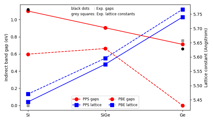
Use then the script plot_pps.py to plot the results.
Running that script should produce the figure shown below,
where the calculated indirect band gaps are shown in red circles,
and the calculated lattice constants are shown in blue squares,
both for PBE (dashed lines) and DFT-PPS (solid lines).
The DFT-PPS band gaps of Si and Ge compare very well to experiments (block dots; from Ref. [4]), and varies roughly linearly with germanium content. On the contrary, the ordinary PBE method predicts zero Ge band gap.
The DFT-PPS lattice constants of pure Si and Ge are also closer to experiments (grey squares) than found with non-corrected PBE.
Manually specifying DFT-PPS parameters
It can be very convenient to manually specify the DFT-PPS projector shift parameters. This may be especially useful in DFT-PPS calculations for elements where there are no default DFT-PPS parameters (only Si and Ge currently have defaults).
The projector shifts are supplied using an instance of the
PseudoPotentialProjectorShift class,
which is then given as an argument to the SG15 basis set.
The following script manually sets the Si and Ge DFT-PPS
parameters identical to the default ones:
#----------------------------------------
# Basis Set
#----------------------------------------
# Basis set for Silicon
SiliconBasis_projector_shift = PseudoPotentialProjectorShift(
    s_orbital_shift=21.33*eV,
    p_orbital_shift=-1.43*eV,
    d_orbital_shift=0.0*eV,
    f_orbital_shift=0.0*eV,
    g_orbital_shift=0.0*eV
    )
SiliconBasis = BasisGGASG15.Silicon_Medium(projector_shift=SiliconBasis_projector_shift)

# Basis set for Germanium
GermaniumBasis_projector_shift = PseudoPotentialProjectorShift(
    s_orbital_shift=14.55*eV,
    p_orbital_shift=0.20*eV,
    d_orbital_shift=-2.17*eV,
    f_orbital_shift=0.0*eV,
    g_orbital_shift=0.0*eV
    )
GermaniumBasis = BasisGGASG15.Germanium_Medium(projector_shift=GermaniumBasis_projector_shift)

# Total basis set
basis_set = [
    SiliconBasis,
    GermaniumBasis,
    ]
Warning
Choosing the appropriate DFT-PPS parameters may be a very delicate matter, and often requires a numerical optimization procedure. The SciPy software offers numerous such routines, but if you choose to use non-default DFT-PPS parameters, the quality of those parameters is entirely your own responsibility as a user!
QuantumATK does not offer support for optimizing DFT-PPS parameters; we recommend in general that users stick to the default parameters, if they exist.