Formation energies and transition levels of charged defects
Version: O-2018.06
In this tutorial you will learn how to calculate the formation energies of neutral and charged point defects, and the transition levels between stable charge states for a given defect centre. Specifically, we will work with the substitution of boron in diamond. We will use the ChargedPointDefect study object, to set up and analyze the calculations.
If you are unfamiliar with this topic, you might also want to consult the introductory tutorial on formation energies, which focuses on bulk systems and neutral defects: Calculation of Formation Energies.
Note
The ChargedPointDefect study object was introduced in the O-2018.06 release, and is the recommended way of studying charged point defects in QuantumATK. Users of previous versions can still do the calculations and analysis in a more complex, and manual, workflow, as described here: Formation energies of charged defects - manual workflow

Procedure for calculating the formation energy
The formation energy \(E^f\) of a defect \(X\) is defined as the energy difference between the investigated system and the components in their reference states. This is analogous to the formation energy of a bulk material, but for charged defects it is less clear how to choose the reference states. Here we follow the procedure outlined in the review by C. Freysoldt et al. [1], originally formualted by Zhang and Nrthrup [2]:
\(E_{tot}[X^q]\) is the total energy of the host crystal with the defect with charge \(q\), which is given in units of the elementary charge (\(e>0\)), \(E_{tot}[bulk]\) is the total energy of the same cell of crystal without the defect, and \(n_i \mu_i\) is the reference energy of \(n_i\) added, or substracted with a change of sign, atoms of element \(i\) at chemical potential \(\mu_i\). The term in parenthesis accounts for the chemical potential of the electron(s) involved in charging the defect. \(E_{VBM}\) is the valence band maximum as given by the QuantumATK band structure calculation for the bulk material of the study (diamond in this tutorial), and \(\mu_e\) is the electron chemical potential defined here with respect to the top of the corresponding valence band. The \(\mu_e\) parameter can then be treated as a free parameter, allowing to account for a shift of the Fermi level, e.g., due to doping. Note that \(\mu_e=E_{gap}/2\) corresponds to the undoped semiconductor case, where \(E_{gap}\) is the intrinsic semiconductor band gap. Finally, \(E_{corr}\) is a sum of relevant correction terms. In our case, it corrects for electrostatic interactions between periodic images of the charged defects and the shift in the electronic bands from the introduction of the defect, using the scheme of Freysoldt et al. [3]. Due to the long-ranged nature of the Coulomb interaction, it can be quite difficult to work with systems that are large enough not to need this correction. The ChargedPointDefect study object allows you to scale the system in an easy way, and see how the formation energy converges with system size. More details of the correction scheme can be found in the Appendix.
In order to calculate the formation energy, we need to compute each of the terms outlined above. The total workflow is listed below:
Select the compound and defect to be investigated, and the computational model to be used (exchange-correlation, pseudopotentials, etc.).
Relax the pristine bulk system using the chosen computational model.
Determine the chemical potential of the elements in the defect. In this case we use the total energy of the bulk for the element added substitutionally.
Setup the undefected supercell to calculate \(E_{tot}[bulk]\) and \(E_{VBM}\).
Introduce the (charged) defect and relax the system to obtain \(E_{tot}[X^q]\).
Calculate the correction terms in \(E_{corr}\) and finally the formation energy.
The latter three, and most complicated items, will be handled by the study object. These three items must also be repeated for each supercell size, and the latter two also for each charge state. In comparison, the first three items must only be done once.
Setting up the calculation
Initial calculations - optimized bulk diamond, dielectric constant and boron chemical potential
We first need to do some small initial calculations, to generate the input structure and the parameters required for the calculation of the formation energies, including corrections:
Optimized structure of diamond
Dielectric constant of diamond
Chemical potential of boron atoms, from bulk boron
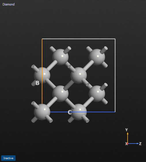
In order to make the interpetration easier when analyzing the results, we will use the cubic/conventional form of the unit cell of diamond. It can be generated from the primitive cell by using the function: tool in the Builder.
We will do the first two calculations in the same script. Set up a script to optimize the geometry of diamond and then calculate the optical spectrum. Use the following changes from default in the script for diamond:
New calculator: k-point density of 4 Å.
Optimize geometry: Untick Constrain lattice vectors and fix fractional coordinates.
Optical Spectrum: k-point density of 12 Å and 100 bands above and below the Fermi level.
For boron, set up a script to optimize the geometry and calculate the total energy. Make the following changes from default values:
New Calculator: k-point density of 4 Å and a density mesh cutoff of 55 Ha.
Optimize geometry: Untick Constrain lattice vectors and fix fractional coordinates.
As the focus of this tutorial is on the ChargedPointDefect study object, you can save time and download the scripts for the preliminary calculations here: bulk-diamond.py and bulk-boron.py. However, if you are unsure of how to do these basic calculations, please see the appropriate tutorials to familiarise yourself with the concepts.
Tip
If you need more guidance on how to set up these calculations, please see these tutorials:
Extracting initial parameters
We get the dielectric constant from the OpticalSpectrum analysis object. Open the OpticalSpectrum  object on the LabFloor in Text Representation, and copy the dielectric function value for the xx-component at zero energy. It should be approximately 6.3.
In this tutorial, we will use bulk boron as the energetic reference for the substitutional boron atom. This means that the chemical potential for boron is the total energy per atom of bulk boron. Open the TotalEnergy  object on the LabFloor in Text Representation, copy the energy value and divide it by 12. The result should be approximately -80.0 eV.
The ChargedPointDefect study object
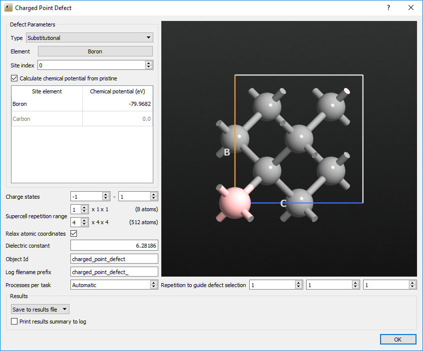
We will now set up the full calculation of the ChargedPointDefect study object. Drag the optimized structure onto the Builder and send it on to the Script Generator. Add a New Calculator and a ChargedPointDefect study object.
The calculator should be set up with the same parameters as used for the geometry optimization of bulk diamond in the previous section. We are now ready to set up the study object:
Change Type from Vacancy to Substitutional.
Change Element from Indium to Boron.
Type in the desired value of the chemical potential for boron, which is -79.96822167 eV in this case.
Change Charge states to -1 as the lower bound and +1 as the higher bound.
Change the upper limit of Supercell repetition range to 4x4x4.
Change the Dielectric constant to 6.28186.
Warning
For substitutional defects, the ChargedPointDefect study object automatically assigns the default pseudopotential and basis set to the substitutional element. In this tutorial, this is what we wish to use, and therefore no additional steps are needed. However, if you wish to use a non-default basis set, you should manually add it to the calculator, either in the Script Generator or in the script.
The window should now look like this:
Save the script and run it on your desired cluster. In our case, it took about 13 hours to run on a total of 32 cores. If you encounter any problems, you can compare your script against the one we have provided here: boron_in_diamond.py
Warning
From the P-2019.03 release the ChargedPointDefect study object was moved to the SMW package. In order to run boron_in_diamond.py with this version it is therefore necessary to add
from SMW import *
at the top of the script.
Tip
The study objects contain automatic restart functionality. If the script does not complete for some reason, simply run it again. It will automatically read the status from the .hdf5-file, and set about completing the remaining tasks.
Analyzing the results
We are now ready to analyze the results of our calculations. Select the ChargedPointDefect  object on the LabFloor. In the right-hand list, open the Defect Analyzer. You should now see a window looking like this:

This is the formation energy for each charge state of the defect, as a function of the chemical potential of the electrons, relative to the valence band maximum. The colored lines each represent a charge state, the solid black line shows the most stable charge state at a given electronic chemical potential, and the dotted lines show the transitions between different charge states. In this case, the +1 state is stable only for very low values of the electron chemical potential, while the neutral state is most stable up to about 0.4 eV. If the electronic chemical potential is higher than that, the -1 charge state is most stable.
On the left, you can choose which supercell to base the plot on, including the extrapolation to infinity, and which charge state to highlight. You can also choose whether or not to include the corrections and whether the black line should be shown or not. On the right, you can change the chemical potentials of the elements.
Charge state -1
We will now look more closely at each of the charge states, starting with the -1 state. Click on the tab titled Finite size scaling. The main panel in the window should now look like this:
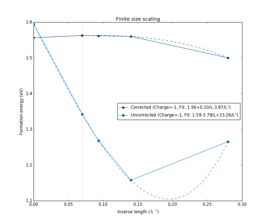
The figure shows the formation energy as a function of the inverse length of the supercell, defined as the the cubic root of the volume. It shows both with the correction terms (dark blue), and without corrections (light blue). In both cases, they are extrapolated to infinite supercell size, with the fits shown as dashed lines. Notice how they both converge to approximately the same formation energy value, and how the formation energy values with the corrections included are already converged to the extrapolated value for the second-smallest 2x2x2 supercell. This shows that this charge state is well-localized within the 2x2x2 supercell, and the correction scheme, which mitigates finite-size effects on the charged defect formation energy, is valid for this particular charged defect state.
Next, click on the tab titled Band shift correction. The window should now look like this:
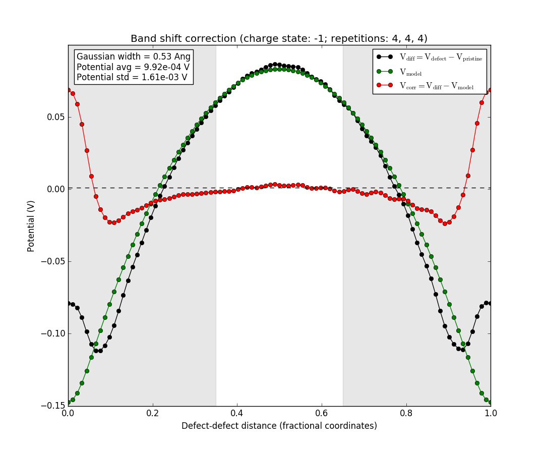
The black line is the difference between the potentials of the supercell with the defect and the pristine supercell without the defect. The green line is the potential from a Gaussian model charge placed at the defect position (the origin of the plot), and the red line is the difference between the two. The light area in the middle is the region where the red line is averaged to produce the value of the band shift term of the correction. The red line should be flat in this region for the correction term to be appropriately calculated. If this is not the case, the assumptions of the correction scheme are violated and it does not apply. In this case, however, the defect charge is well-localized and the red line is flat in the region where the bandshift is evaluated.
You may also select the other supercell sizes, and see how the defect charge is well-behaved, even for the 2x2x2 supercell. However, it is not well-localized for the very smallest 1x1x1 supercell, as expected. This supercell is much too small to give sensible results, even with the correction sceheme, and is included here only for comparison.
This behavior is not surprising, as the boron atom has one less (valence) electron than carbon atoms. Therefore, the -1 charge state leads to the boron atom being electronically equivalent to a carbon atom, stabilizing it as a substitutional defect.
Charge state 0
We now move on to the neutral defect. Go again to the Finite size scaling tab, and change the charge state to 0. Select also the 4x4x4 supercell if you have changed away from that. The window should now look like this:
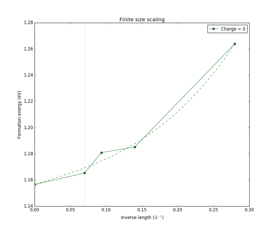
Note that there is now only one data-set, as the corrections only apply if the system is charged. We see also that the variation in formation energy with size is significantly smaller than before. Here, the total range is about 0.1 eV, compared with 0.4 eV before. This is expected, as the neutral defect has no explicit charge that can suffer from finite-size effects. However, there can still be, e.g., elastic interactions between the defects, and it is therefore expected to see some size dependence, as we do here.
For completeness, we will take a short look at the Band shift correction tab. Click it, and the window should now look like this:
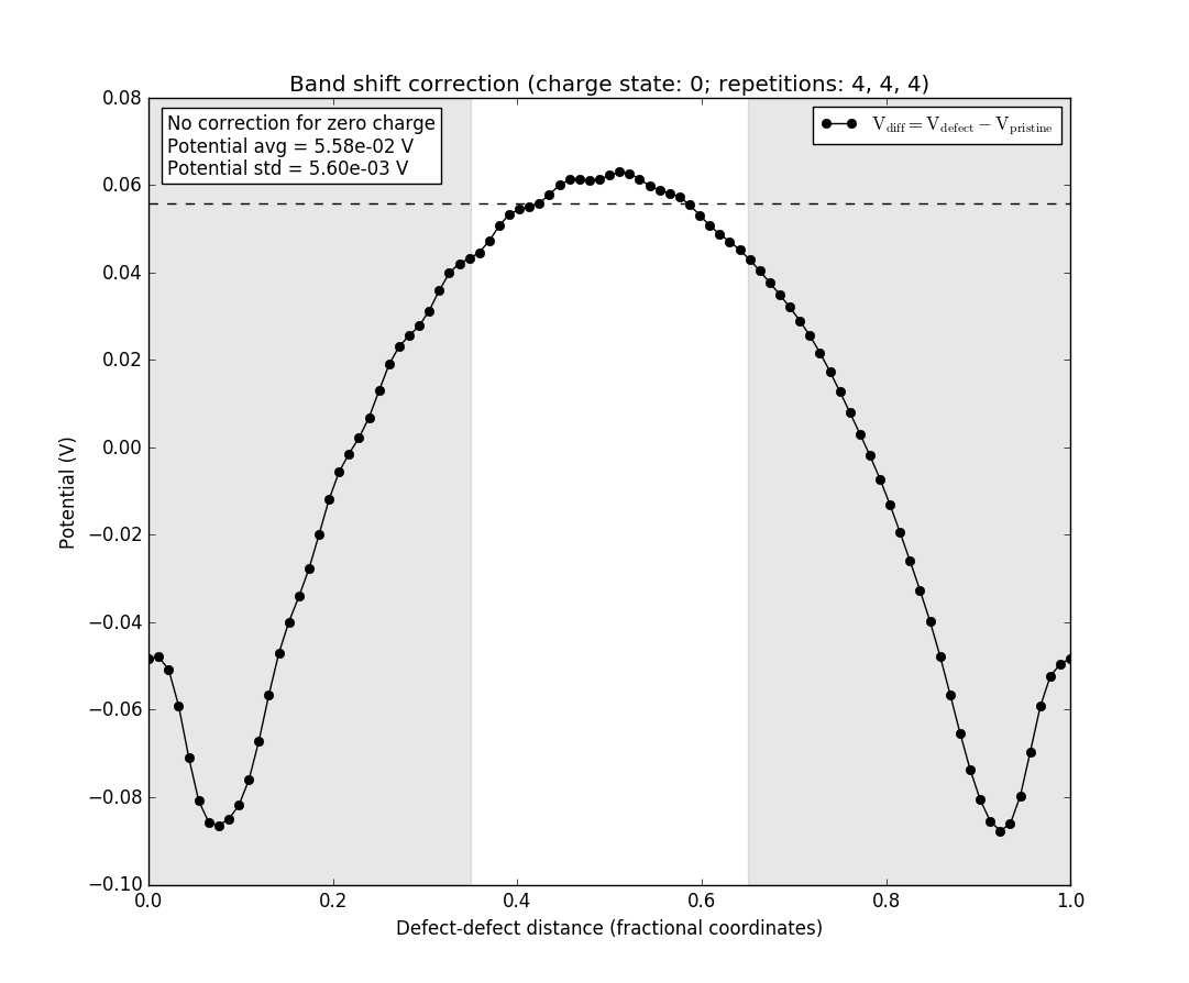
Only the black line is present as there is no charge to model, and hence no difference to investigate. Note also the box in the upper left, which informs that there is no correction for the neutral defect.
Charge state +1
Finally, we turn our attention to the +1 charge state. Select again the Finite size scaling tab, and change the charge state to +1. Select also the 4x4x4 supercell if you have changed away from that. The window should now look like this:
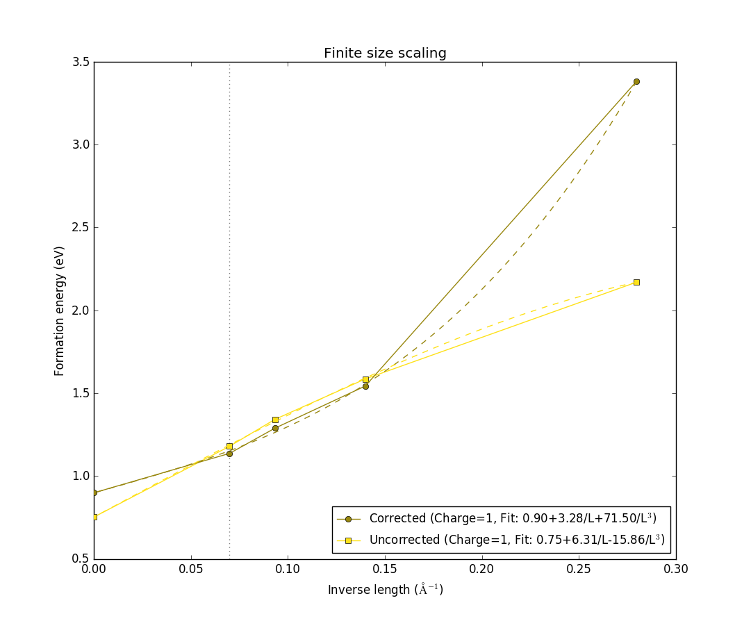
In this case it is very hard to see at first glance which data-set is the raw data and which includes the corrections, in contrast to what we saw for the -1 charge state. They still seem to converge to approximately the same value, but the corrections do not really add any useful information in this case. This indicates either a defect that cannot be modelled using the correction scheme, or a defect that is simply unphysical. In both cases, it will often be a delocalized charge. In order to look further at this charge state, select the tab Band shift correction again. The window should now look like this:
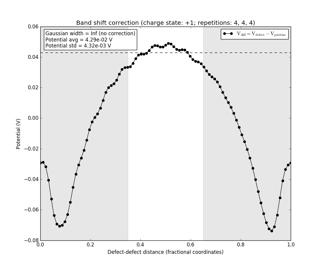
Note the box in the upper left again. We see that the Gaussian width is described as infinite, and no corrections are therefore applied, as they require a finite width of the charge distribution.
In this case, the best approach is to use as large a supercell as possible, removing the need for corrections and the accompanying approximations and assumptions.
Discussion and summary
Boron is a p-type dopant in group-IV semiconductors such as diamond. As mentioned above, this is because boron has one less valence electron than carbon, and so its effect as a substitutional defect in the diamond lattice is to add an effective positive charge (i.e., a hole) to the crystal. This also makes boron an acceptor dopant, as it will attract an electron from the crystal to completely fill its covalent bonds with its neighbours in the lattice.
When the neutral boron dopant captures an electron it becomes ionized. The ionization energy is readily measured experimentally, and corresponds to the stable-charge transition level between the 0 and -1 charge states shown in the main plot of the Defect Analyzer. The experimental value is 0.37 eV [4], in good agreement with our calculated value of 0.4 eV.
The +1 charge state, instead, is not experimentally relevant; this is again confirmed by our results, which show it to be almost completely absent as a stable charge state within the band gap, as the transition level between +1 and 0 is close to the valence band maximum.
In this tutorial, we have used the ChargedPointDefect study object to set up and analyze a calculation of the formation energies for various charge states of boron substitution in diamond. QuantumATK includes a correction scheme that can mitigate the errors due to periodic interaction between the defects in finite supercells, if the defect is well-localized. In general, and especially if the defect charge is not well-localized, charged defects are best studied with larger supercells, and we have seen how the convergence with respect to size can be studied.
Appendix
The periodic correction scheme
As already mentioned, we use the correction scheme proposed by Freysoldt et al. [3] to correct for the electrostatic interaction between the periodic images of the charges and the band shift caused by introduction of the defect. This correction contains two terms:
where \(E_{lat}\) corrects for the interaction between the periodic images of the charge and \(q \Delta V_{q/b}\) corrects for the band shift. \(E_{lat}\) is calculated by considering the electrostatics of a model charge distribution, which is fitted to the actual calculation by the study object, and comparing the potential in the periodic cell with the potential where the boundary conditions are not periodic:
\(V_q^{lr}\) is the long-range potential of the model charge distribution and \(\tilde{V}_q^{lr}\) is the corresponding quantity in the periodic cell and shown in green. \(\Delta V_{q/b}\) is calculated from the shift in the electrostatic potential due to introduction of the defect:
where \(\tilde{V}_{q/b}\) is the difference between the electrostatic potential in the pristine bulk configuration and with the defect added and shown in black. \(\Delta V_{q/b}\) is shown in red, and should be evaluated far from the defect, where it is constant, in order to get the correct offset in the zero-point reference energy . This is shown by the lightly colored region in the plots above.
Note that the obtained difference is defined between two screened potentials, see the reference [3]. The dielectric screening is described by the static dielectric constant computed in the preliminary calculations.