Complex band structure of Si(100)
Version: X-2025.06-SP1
In this tutorial, you will calculate the complex band structure of a Silicon crystal along the (100) direction [1].
In particular, you will:
Create a unit cell of bulk Silicon by cleaving the Silicon crystal in (100) direction.
Set up and run the calculation.
Plot and visualize the complex band structure.

Background
In a periodic solid, the eigenstates \(\psi_{n{\bf k}}\) of the Schrödinger equation \(H \psi_{n{\bf k}} = E_{n{\bf k}} S \psi_{n{\bf k}}\), (\(S\) is the overlap matrix) are the Bloch states that can be written as \(\psi_{n{\bf k}}({\bf r}) = e^{-i {\bf k}\cdot {\bf r}} U_{n{\bf k}}({\bf r})\), where \(U_{n{\bf k}}({\bf r})\) is a periodic function with the same periodicity as the crystal itself. In a usual band structure calculation, the wave vector \({\bf k}=(k_x, k_y, k_z)\) components are real number, and by solving the above Schrödinger equation for various fixed values of \({\bf k}\)-vector components (typically corresponding to symmetry lines in the first Brillouin zone) an eigenproblem is defined, from which the eigenenergies \(E_{n{\bf k}}\) (i.e., the band structure) can be determined.
When calculating the complex band structure, the eigenproblem is formulated differently [1]. For a crystallographic direction given by the reciprocal lattice vector, \({\bf g}_C\), the corresponding eigenvalue problem is solved with respect to the \(k_C\) component of the \({\bf k}=(k_A, k_B, k_C)\) vector for a fixed energy (\(E\)) and \((k_A, k_B)\) components of the \({\bf k}\) vector.
Given this formulation of the eigenproblem, the resulting solutions will correspond, in general, to complex eigenvalues \(k_C = Re(k_C) + i Im(k_C)\), which can be divided into 4 groups of solutions:
The solutions with real eigenvalues \(k_C = Re(k_C)\) (and \(Im(k_C)=0\)) correspond to the propagating states, which are the Bloch states obtained in a usual band structure calculation as described in the previous paragraph.
The solutions with imaginary eigenvalues \(k_C = i Im(k_C)\) (and \(Re(k_C)=0\)) correspond to the evanescent states, which are either decaying or growing exponentially in the crystallographic direction given by the \({\bf g}_C\) vector.
The solutions with general complex eigenvalues \(k_C = Re(k_C) + i Im(k_C)\) (and \(Re(k_C) \& Im(k_C) \ne 0\)) also correspond to the evanescent states decaying or growing, but in an oscillatory manner.
There is also a specific type of solutions (evanescent states) with complex eigenvalues having \(Re(k_C)\) at the Brillouin zone edge, \(k_C = \pi/L + i Im(k_C)\), where \(L\) is the distance between two adjacent atomic layers in the crystallographic direction given by the \({\bf g}_C\) reciprocal lattice vector [1].
The evanescent solutions (2)(4) do not correspond to physical electronic states in an infinite, perfect crystal, unlike the propagating solutions of type 1 corresponding to the usual band structure (Bloch states). However, if a surface or interface system has localized electronic states, some of the evanescent solutions obtained in complex band structure calculation of the corresponding bulk material(s) forming the surface (or interface) would then describe the actual physical localized electronic states in the region away from the surface (or interface) plane.”
Note
You will primarily use the graphical user interface QuantumATK for setting up and analyzing the results. If you are new to QuantumATK, it is recommended to go through the Introductory Tutorials.
The calculations in this tutorial will be performed using the semi-empirical models of QuantumATK. A complete description of all the parameters, and in many cases a longer discussion about their physical relevance, can be found in the SemiEmpiricalCalculator manual. In particular, the reference manual entry for complex band structure calculation is of relevance: ComplexBandstructure.
Si crystal cleaved in (100) direction
Start QuantumATK and create a new project named “ComplexBandstructure”. Then go to
Builder via  icon, and follow the next step:
Click on
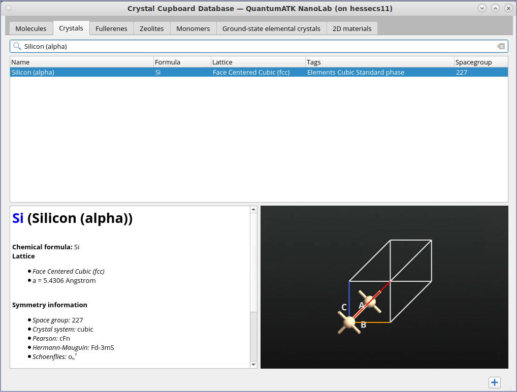
 icon in the Stash, and select From Database
  .
.Search for “Silicon (alpha)” structure in the Search box.
Double-click the line to add the structure to the Stash, or click the
icon in the lower right-hand corner.
Search for “Surface (Cleave)” in the right-hand side Panel of the Builder. Open it and follow the next steps to set up the Si(100) surface:
Keep the default Miller indices (100) and click Next.
Keep the default lattice vectors and click Next.
Select Periodic (bulk-like) for the out-of-plane cell vector.
Set the thickness of the surface to 1 layer.
Click Finish to add the (100) cleaved Si structure to the Stash.
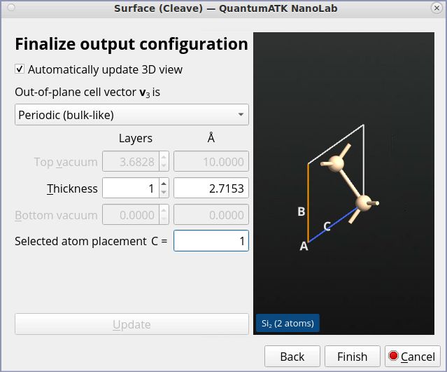
With these settings we use a surface representation with a minimum number of layers in order to reduce the calculation time and avoid zone folding.
Note
The QuantumATK convention is that the cleave plane – in the present tutorial cleaved in the (100) direction of Silicon crystal – is spanned by the two lattice vectors, \({\bf A}\) and \({\bf B}\). In the “electrode” mode, the normal to this plane coincides with the direction given by the third lattice vector, \({\bf C}\), but in the “bulk-like” mode this does not need to be the case for a general crystal. Thus, QuantumATK ComplexBandstructure object calculates the complex band structure always along the third reciprocal lattice vector, \({\bf g}_C\), which is parallel to the \({\bf A} \times {\bf B}\) vector, also meaning that the \({\bf g}_C\) vector is perpendicular to the \({\bf AB}\) plane. Given the selected unit cell structure of Silicon, you will, therefore, obtain the complex band structure along the (100) crystallographic direction, which is aligned with the \({\bf g}_C\) vector.
Complex band structure calculation
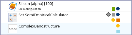
Send the structure to Workflow Builder ( )
using the
)
using the  icon in the lower right-hand corner of the
Builder, and follow the next steps:
icon in the lower right-hand corner of the
Builder, and follow the next steps:
Add a
 Set SemiEmpiricalCalculator block.
Add the
 Analysis –> ComplexBandStructure block.
Change the default output filename to
si_100_cbs_results.hdf5.
Next, open the inserted Set SemiEmpiricalCalculator block
(double-click it), and set up a semi-empirical calculation:
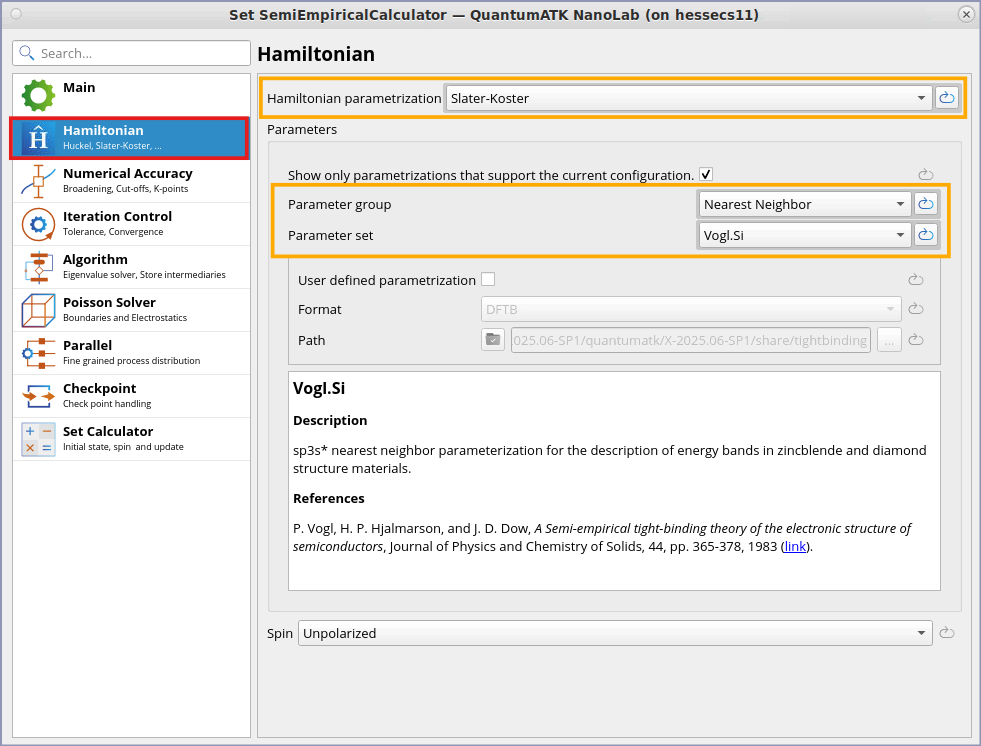
Select Hamiltonian as Slater-Koster.
Set the k-point sampling to 4x4x4.
Ensure that the default values of Parameter group is Nearest Neighbor and Parameter set is Vogl.Si.
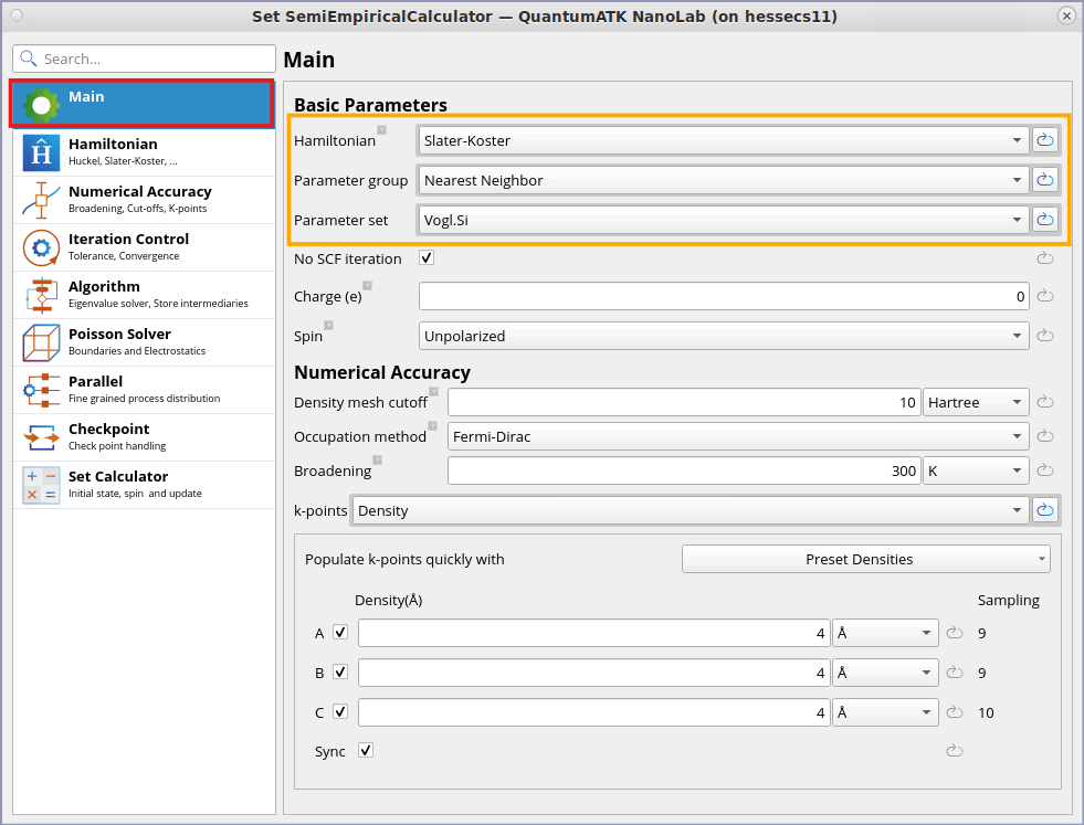
You can find more detail about Vogl.Si Parameter set from the Hamiltonian tab:
Close the dialogue by clicking on
 icon in the top right-hand corner.
Next, open the  ComplexBandstructure analysis block, and edit it:
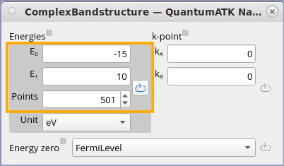
Set the energy range to -15 to 10 eV with 501 points.
Note
The projection of \({\bf k}\) on the cleave \({\bf AB}\) plane is kept constant in the complex band structure calculation, and the value of the projection is specified by the \((k_A,k_B)\) parameters, which are given in units of the two first reciprocal lattice vectors, \({\bf g}_A\) and \({\bf g}_B\). Therefore, the obtained solutions will lie along the third reciprocal lattice vector, \({\bf g}_C\), which is parallel to the cleave plane normal. A new set of solutions \(k_C+i\kappa_C\) is obtained for each value of \((k_A,k_B)\).
The current widget does not plot the real part of the complex eigenvalue solutions of type 3. Only the real part of the real eigenvalue solutions of type 1 (related to Bloch states), and the imaginary part of the complex eigenvalue solutions of type 2, 3, and 4 (related to evanescent states) are plotted in the widget. Please note that \(k_C\) is therefore the real part of the complex band structure, while \(\kappa_C\) is the complex part.
You have succesfully created a workflow for complex band structure calculation. Now, click on
icon and submit the Jobs as script  . It should only take a
few minutes for this small system.
. It should only take a
few minutes for this small system.
You can also check the script generated by workflow by sending it to Editor  using . If needed, you can also download the script here:
 si_100_cbs.py.
Tip
This type of calculation parallelizes extremely well, so for larger structures it is warmly recommended to execute the script in parallel.
Analysing the results
The file si_100_cbs_results.hdf5 should now have appeared on the QuantumATK  Data View.
It contains the saved Slater-Koster calculation and the ComplexBandstructure
analysis object:
Data View.
It contains the saved Slater-Koster calculation and the ComplexBandstructure
analysis object:
ComplexBandstructure
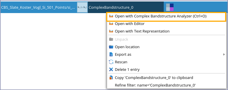
Select
si_100_cbs_results.hdf5file in Data Source.Select ComplexBandStrucure analysis object in
Data View.Double-click on it, or right-click on it and select Open with Complex Bandstructure Analyzer (Ctrl+O).
A window with a plot of the complex band structure will pop up.
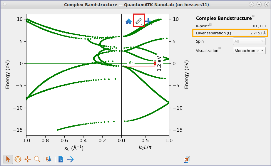
Fig. 44 Si(100) band structure. The right-hand part of the plot shows the real bands – note the indirect band gap of ~1.2 eV. The left-hand part of the plot shows the complex bands, plotted against the imaginary part, \(\kappa_C\). The bands with a small imaginary part are the most important ones, since they are less damped if you should try to tunnel electrons through a thin slice of Silicon in the (100) direction.
Note
In the plot above, the solutions \(\kappa_C\) are given in reciprocal Cartesian coordinates, to make it easier to compare different structures. For the real part of the band structure, on the other hand, the solutions \(k_C\) are normalized by \(L\), the layer separation perpendicular to the cleave plane. In the case of a fcc crystal cleaved along (100), the layer separation is \(L=a/2\), where \(a\) is the lattice constant. The layer separation is reported in the plot.
Another way to visualise the real part of the complex band structure is using
colors. In the plot window, select the visualzation as Color. Please note that the
default color template may be different from the one shown below. In order to get the same color
template, you can change the color map to rainbow in the Plot Editor using
Edit  icon.
icon.
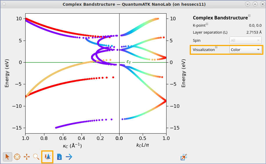
Fig. 45 2D visualization of complex band structure. Note how the color coding of the k-values applies both to the real and the complex parts of the band structure, which makes it easier to see where the complex bands are attached to the real ones.
The “forest” of complex bands with a rather large value of \(\kappa\) are not usually seen in Slater-Koster calculations. However, for DFT and Hückel, the basis sets are larger, so there are more complex bands as well, connecting unoccupied levels with various valence bands.
3D visualizations
In the complex band structure, there are complex eigenvalues (type 3) with non-zero real part.
Thus, they could be visualized in a three-dimensional
plot, \((x,y,z)=(k_C, \kappa_C, E)\). This is possible with the
following script. Open the QuantumATK Editor and copy-paste
the script and save it as 3D_plot.py. Make sure that the indentation
is correct. Alternatively, you can simply download it here: 3D_plot.py.
 1from QuantumATK import *
 2from mpl_toolkits.mplot3d import Axes3D
 3import matplotlib.pyplot as plt
 4import math
 5
 6# Read the complex bandstructure object from the NC file
 7cbs = nlread('si_100_cbs_results.hdf5', ComplexBandstructure)[-1]
 8energies = cbs.energies().inUnitsOf(eV)
 9k_real, k_complex = cbs.evaluate()
10L = cbs.layerSeparation()
11
12fig = plt.figure()
13ax = fig.add_subplot(111, projection='3d')
14
15# First plot the real bands
16kvr = numpy.array([])
17e = numpy.array([])
18
19# Loop over energies, and pick those where we have solutions
20for (j, energy) in enumerate(energies):
21    k = k_real[j]*L/math.pi
22    if len(k)>0:
23        e = numpy.append(e,[energy,]*len(k))
24        kvr = numpy.append(kvr,k)
25
26# Plot the bands with red
27ax.scatter([0.0,]*len(kvr), kvr, e, c='r', marker='o', linewidths=0, s=10)
28
29# Next plot the complex bands
30kvr = []
31kvi = []
32e = []
33
34# Again loop over energies and pick solutions
35for (j, energy) in enumerate(energies):
36    if len(k_complex[j])>0:
37        for x in numpy.array(k_complex[j]*L/math.pi):
38            kr = numpy.abs(x.real)
39            ki = -numpy.abs(x.imag)
40            # Discard rapidly decaying modes which clutter the plot
41            if ki>-0.3:
42                e += [energy]
43                kvr += [kr]
44                kvi += [ki]
45
46# Plot the complex bands with blue
47ax.scatter(kvi, kvr, e, c='b', marker='o', linewidths=0, s=10)
48
49# Put on labels
50ax.set_xlabel('$\kappa$ (1/Ang)')
51ax.set_ylabel('$kL/\pi$')
52ax.set_zlabel('Energy / eV')
53
54plt.show()
Execute the script using the Job Manager or from
a terminal. The plot will resemble the figure below, but your points will
be more scattered, since the figure below was produced from a Slater-Koster
calculation with 10,001 energy points instead of 501.
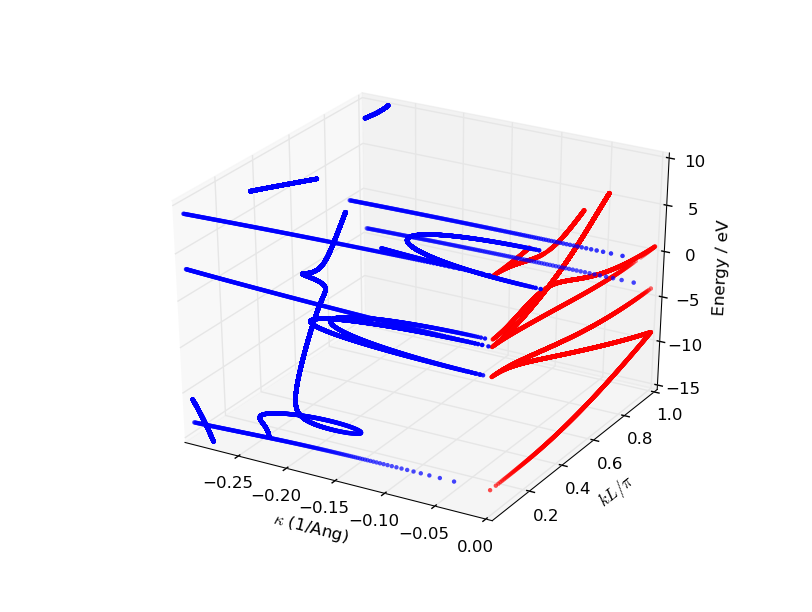
Fig. 46 3D visualization of the complex band structure of Si(100). The real bands are plotted with red dots and the complex part in blue. Note how the complex bands connect with the real bands.
Hint
One may see that there are “gaps” in the complex band structure visualization. To fill the “gaps”, one would have to increase the number of energy points for better sampling of the energy axis, since the actual calculation of the complex band structure assumes calculating \({\bf k}\) vs. \({\bf E}\), i.e., \({\bf k}={\bf k}({\bf E})\), unlike the usual band structure calculation where one calculates \({\bf E}\) vs. \({\bf k}\), i.e., \({\bf E}={\bf E}({\bf k})\).