Bi2Se3 topological insulator
Version: 2016.2
Topological insulators are electronic materials that have a bulk band gap like an ordinary insulator, but still support conducting states on their surface. It can be shown that these states are topologically protected due to a non-trivial topological index of the material and cannot be removed by any distortions. The 2D energy–momentum relation of these surface states has a “Dirac cone” structure similar to that of graphene. Topological insulators therefore constitute a new class of quantum matter governed by exotic physics that may some day be exploited in electronic devices. Refs. [1] and [2] provide recent reviews of this highly active field of research.
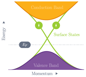
Fig. 38 The valence and conduction bands of a topological insulator are separated by a non-zero band gap, but bands due to surface states cross the band gap and lead to electronic conduction at the surface of the material.
In this tutorial you will learn how to use ATK-DFT to study the Bi2Se3 compound, which is a 3D strong topological insulator. Nonequilibrium Green’s function DFT calculations were recently reported for a Bi2Se3 thin film connected to leads in a two-terminal device setup [3]. However, this tutorial focuses on bulk calculations and properties of the surface states. In particular, you will:
Use the QuantumATK Crystal Builder to construct the Bi2Se3 crystal structure.
Investigate the bulk Bi2Se3 band structure with and without the SOC.
Construct a Bi2Se3 slab configuration and compute the SOC band structure, which exhibits the surface states mentioned above.
Compute the density of states (DOS) around the Fermi energy, which nicely illustrates the Dirac cone inside the bulk band gap.
Investigate the surface state penetration depth into the material.
Plot the spin-resolved Fermi surface of surface states, and investigate how the in-plane spin orientation varies on the Fermi surface.
Calculate the topological invariants for Bi2Se3.
Note
It is essential to include the spin-orbit coupling (SOC) to correctly describe the electronic structure of a topological insulator.

Build the Bi2Se3 crystal
Open the QuantumATK Builder  and click
. As described
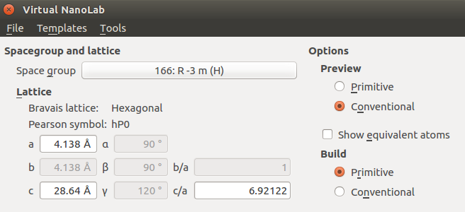
in [4], the Bi2Se3 crystal is rhombohedral and
belongs to space group \(\mathrm{R \overline{3} m}\). It has lattice
constants a=4.138 Å and c=28.64 Å, and internal coordinates \(\mu\)=0.399 for Bi sites and \(\nu\)=0.206 for Se sites. The basic
Bi2Se3 unit cell, called a quintuple layer (QL), contains 5 atoms:
One Se atom at coordinate (0, 0, 0), Bi atoms at internal coordinates
\((\pm\mu,\pm\mu,\pm\mu)\), and Se atoms at
\((\pm\nu,\pm\nu,\pm\nu)\).
and click
. As described
in [4], the Bi2Se3 crystal is rhombohedral and
belongs to space group \(\mathrm{R \overline{3} m}\). It has lattice
constants a=4.138 Å and c=28.64 Å, and internal coordinates \(\mu\)=0.399 for Bi sites and \(\nu\)=0.206 for Se sites. The basic
Bi2Se3 unit cell, called a quintuple layer (QL), contains 5 atoms:
One Se atom at coordinate (0, 0, 0), Bi atoms at internal coordinates
\((\pm\mu,\pm\mu,\pm\mu)\), and Se atoms at
\((\pm\nu,\pm\nu,\pm\nu)\).
Lattice
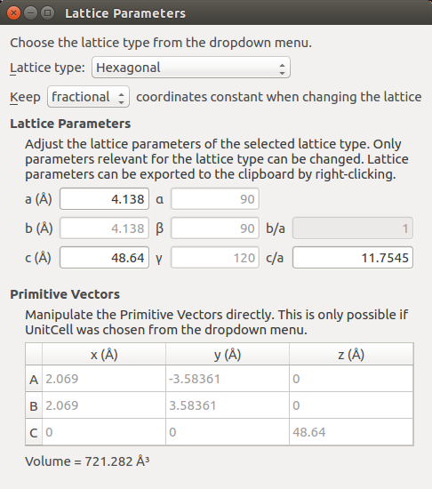
In the Crystal Builder, choose the Trigonal space group number 166 with Hexagonal setting, and enter the lattice parameters:
Basis
Then specify the atomic basis with which to decorate the lattice, i.e. enter the internal coordinates of the unique sites of the Bi2Se3 crystal and the elements that should be at those sites:
Click the
 icon and select site 3a: (0,0,0), and change
the element from hydrogen to selenium.
icon and select site 3a: (0,0,0), and change
the element from hydrogen to selenium.Use the same procedure twice for specifying the remaining sites, but choose 6c: (0,0,z) for the site type, and enter the internal coordinates z=0.399 for bismuth and z=0.206 for selenium.
The Crystal Builder window should now look like illustrated below. Click Build to build the bulk configuration – it will then appear in the Builder Stash.
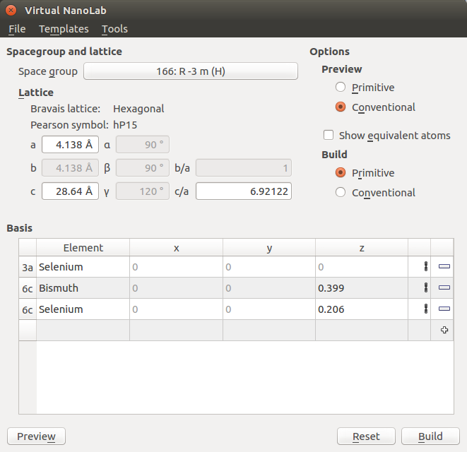

You have now built the Bi2Se3 bulk configuration with 3 QLs and 15
atoms in total. Continue to the next section to start doing some DFT
calculations for this material. If needed, you can also download the
bulk configuration here: Bi2Se3_bulk_configuration.py
Bi2Se3 bulk band structure
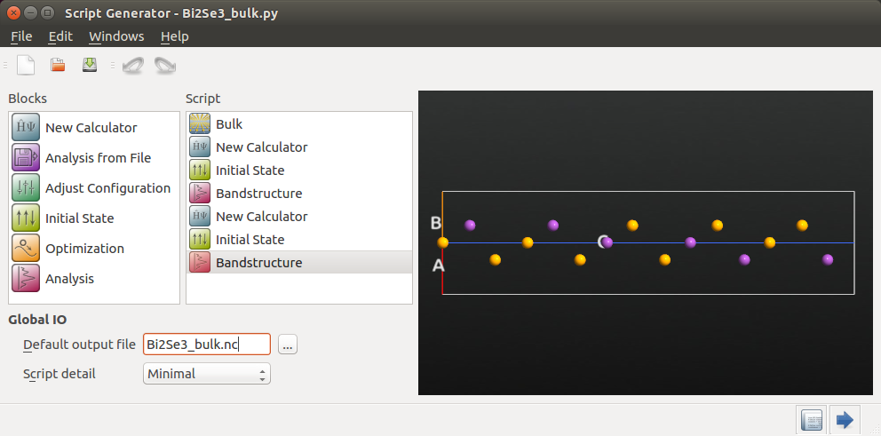
Send the bulk configuration to the Script Generator, and set up a Python script that uses ATK-DFT to calculate the band structure with and without the spin-orbit coupling. The script should first calculate the self-consistent GGA state and perform band structure analysis, and then use that state as an initial guess for the self-consistent SOGGA state, again followed by band structure analysis.
The Script Generator now contains the bulk configuration. Add the
 New Calculator,
  , and
, and  Initial State blocks, as illustrated below. Also change the default
output file to
Initial State blocks, as illustrated below. Also change the default
output file to Bi2Se3_bulk.nc.
GGA calculation
Open the first New Calculator block to edit it:
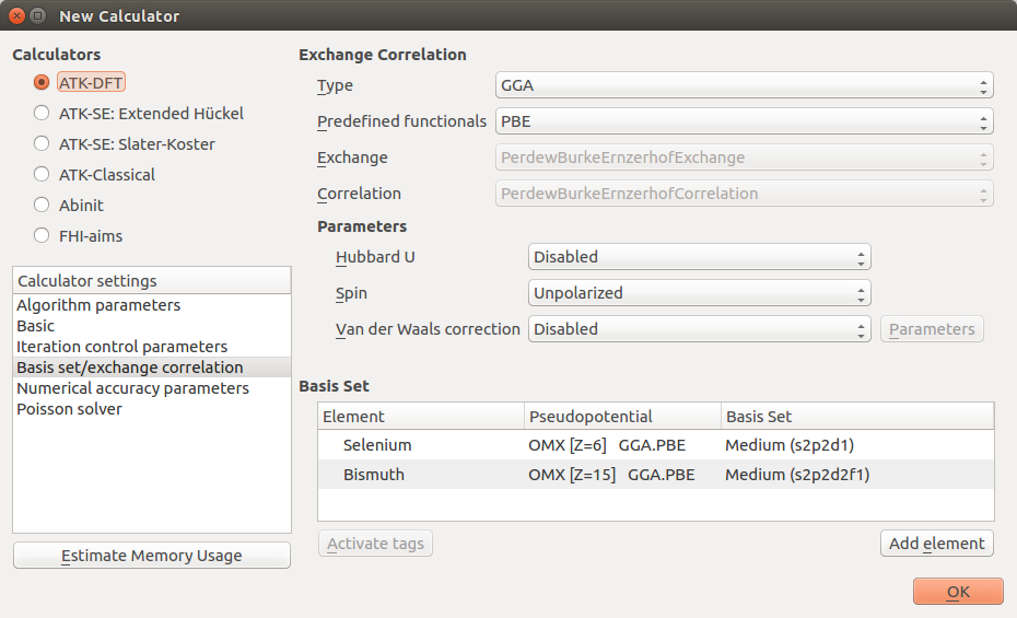
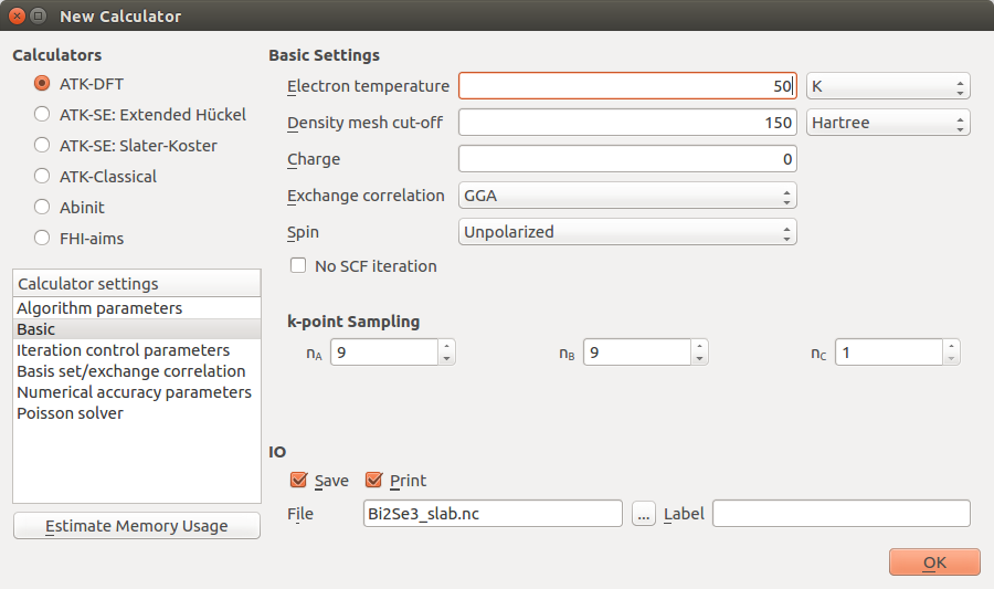
Make sure to choose the ATK-DFT calculator.
In the Basis set/exchange correlation settings, choose GGA and change the pseudopotentials to the OMX family with Medium basis sets for both Se and Bi.
In the Basic settings tab, increase the density mesh cut-off to 150 Hartree, and set up a 9x9x3 k-point grid. Click OK to save the settings.

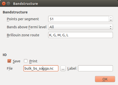
Then open the first Bandstructure block and edit it:
Increase points per segment to 51 to get a nicely resolved band structure.
Change the Brillouin zone route to K, G, M, G, L.
Change the IO file to
bulk_bs_gga.nc.

SOGGA calculation
Open the second New Calculator block, and edit it
such that the settings are identical to those in the first calculator,
but set the Spin parameter to Noncollinear Spin-Orbit in order to
do a SOGGA calculation. Remember to also set the pseudopotentials,
density cut-off, and k-points.

Next, open the second Initial State block, and
select User spin for Initial state type, tick the Use old calculation
option, and enter the file name Bi2Se3_bulk.nc from which the
GGA state should be read.

Finally, set up the second Bandstructure block identically
to the first one, but use bulk_bs_sogga.nc for the IO file.
Results
The Python script is now ready. Save it as Bi2Se3_bulk.py.
If needed, you can also download it here: Bi2Se3_bulk.py
Execute it using the Job Manager  or in a Terminal.
The job will take a while, but the wall time can be brought down to
around 40 minutes if executed in parallel with 2 MPI processes on 2 CPUs.
Note that this requires in total about 15 GB of available memory!
or in a Terminal.
The job will take a while, but the wall time can be brought down to
around 40 minutes if executed in parallel with 2 MPI processes on 2 CPUs.
Note that this requires in total about 15 GB of available memory!
Tip
The tutorial Basic QuantumATK Performance Guide offers tips on QuantumATK performance, including how to deal with memory issues.
Once the calculation has finished, the QuantumATK LabFloor contains three sets of data: Bi2Se3_bulk, bulk_bs_gga, and bulk_bs_sogga. The last two contain the GGA and SOGGA band structures. Highlight both band structure objects, and use the Compare Data plugin to plot both of them.

The plot is shown below. Including spin-orbit coupling in the calculations (SOGGA) has a significant impact on the band structure, and widens the direct band gap at the \(\Gamma\)-point However, we do not see any bands crossing the Fermi level (the smallest SOGGA band gap is 0.3 eV), so the Bi2Se3 bulk material is an insulator.

Fig. 39 Comparison of the GGA (blue) and SOGGA (green) band structures of bulk Bi2Se3.
Bi2Se3 surface: Spin-orbit band structure
You will now create a Bi2Se3 slab configuration, and compute the SOGGA band structure, which will exhibit the topologically protected surface states crossing the band gap around the \(\Gamma\)-point.
Constructing the surface
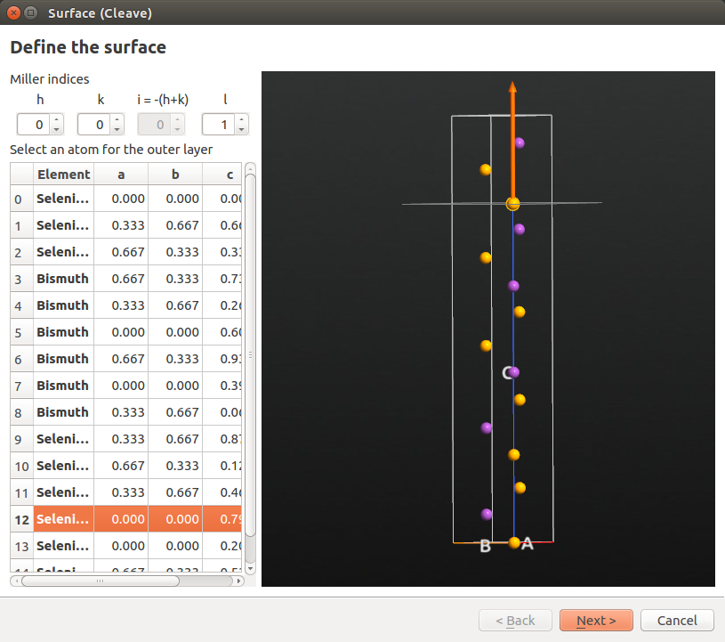
Back in the Builder, highlight the Bi2Se3 bulk configuration (named Crystal), and open the plugin. Choose Miller indices (0001), and select selenium atom #12 as the top atom in the slab. Then click Next.
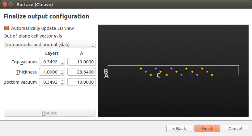
Leave settings at defaults in the “Define surface lattice” options window. In the “Finalize output configuration” options, choose a Non-periodic and normal (slab) out-of-plane cell vector, and enter 10 Å for both top and bottom vacuum. Then click Finish.
The slab configuration, named Crystal (0001), has now appeared in the Stash. As a final touch, highlight the item and use the plugin to convert the lattice type to Hexagonal while keeping the fractional coordinates constant:
DFT-SOGGA calculations
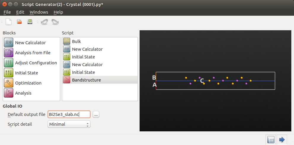
You can now send the slab configuration to the Script Generator, and set up the SOGGA band structure calculation similarly to what you did above for the bulk, but with slight changes:
You will not need the GGA band structure analysis.
Use
Bi2Se3_slab.ncas default output file.Use a 9x9x1 k-point grid (the slab is not periodic along the C-direction).
Decrease the electron temperature from 300 to 50 K. This will improve the DFT description of electron occupations close to the Fermi level.
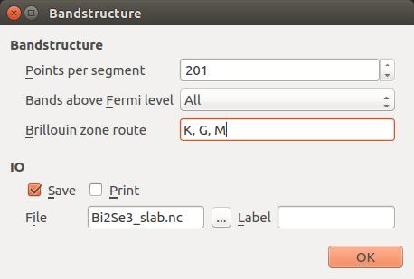
Use 201 points per segment for the SOGGA band structure analysis, and the K–G–M Brillouin zone route.
Alternatively, you can simply skip the above and go directly to the next section to use a pre-made Python script with a few additional features.
Convenient Python script
Click here: Bi2Se3_slab.py to download a Python script that was made
using the procedure outlined above, but also has a few extra features:
The “MemoryUsage” functionality is used to estimate the memory required for the GGA and SOGGA calculations immediately before they are executed.
The SOGGA calculator is constructed as a copy of the GGA calculator, and is then modified accordingly.
A special density mixing algorithm is used for the non-collinear calculation.
Run the calculation using the Job Manager or in a
Terminal. The job will take roughly 30 minutes if executed in 2 parallel
MPI processes on 2 CPUs.
Hint
If you look at the log file during the calculation, you will see that the estimated peak memory requirements are 756 MB per MPI process for the GGA calculation, and 3.8 GB per MPI process for the SOGGA calculation. These are estimates, and in practice you should expect the full calculation to require almost 5 GB per MPI process.
GGA:
+----------------------------------------------------------+
| Memory usage estimate                                    |
| -------------------------------------------------------- |
| Base: Sparse matrices                          44 Mbyte  |
| Base: GridTool+Basis set                      100 Mbyte  |
| Base: SCF history                             442 Mbyte  |
| Base: NLEngine                                 70 Mbyte  |
| Base: Grid terms                               39 Mbyte  |
| Sum of the base terms                         696 Mbyte  |
| -------------------------------------------------------- |
| Peak: Diagonalization                          60 Mbyte  |
| Peak: Grid terms                               19 Mbyte  |
| -------------------------------------------------------- |
| Estimated Peak memory requirement             756 Mbyte  |
+----------------------------------------------------------+

SOGGA:
+----------------------------------------------------------+
| Memory usage estimate                                    |
| -------------------------------------------------------- |
| Base: Sparse matrices                         272 Mbyte  |
| Base: GridTool+Basis set                      100 Mbyte  |
| Base: SCF history                            2726 Mbyte  |
| Base: NLEngine                                 70 Mbyte  |
| Base: Grid terms                              157 Mbyte  |
| Sum of the base terms                        3326 Mbyte  |
| -------------------------------------------------------- |
| Peak: Diagonalization                         446 Mbyte  |
| Peak: Grid terms                               58 Mbyte  |
| -------------------------------------------------------- |
| Estimated Peak memory requirement            3772 Mbyte  |
+----------------------------------------------------------+
Results
The QuantumATK LabFloor should now contain the results of the calculation. Select the band structure object, and use the Bandstructure Analyzer to plot it.

The calculated band structure of the Bi2Se3 slab is shown below. Bands are now present around the Fermi level at the \(\Gamma\)-point – these are surface states. There are four such surface states crossing the Fermi level (indicated by red dots); bands 142 and 143 form a single degenerate band immediately below the Fermi energy, while bands 144 and 145 form a degenerate band above EF. The bulk valence bands are below those surface states (indicated by blue dot). It is clear that the dirac cone is located inside the bulk band gap. There is a tiny gap between the valence and conduction surface bands of size 7 meV. This is a finite size effect from the use of a slab model, which arise from the interaction of the surface bands on opposite sides of the slab. For a larger slab the gap will be reduced.
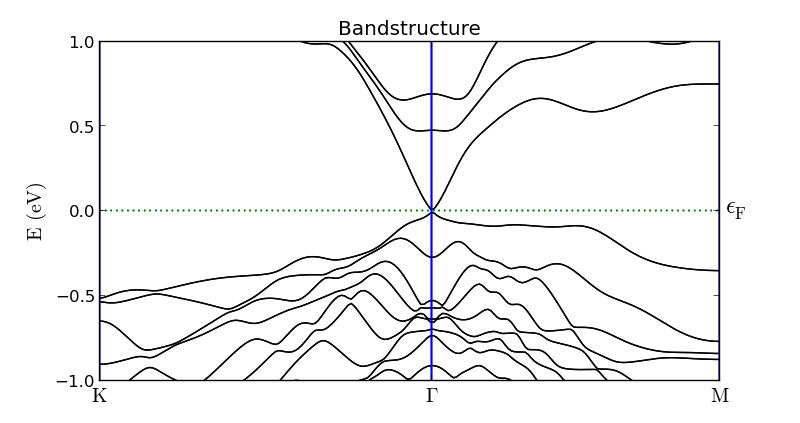

Fig. 40 SOGGA bandstructure of the Bi2Se3 slab configuration. The bottom panel is a zoom-in on the topologically protected Dirac cone. Both surface state bands (red dots) are both doubly degenerate and are located above the bulk valence bands (blue dot).
DOS analysis: Dirac cone finger print
As stated in the introduction, the electronic structure of the surface states close to the Fermi level resembles that of a Dirac cone, where the electron momentum depends linearly on the energy. Since the surface states are the only states present inside the bulk energy gap, we should expect the electronic density of states close to EF to be linear. It is easy to compute and plot the DOS as a post-SCF analysis:
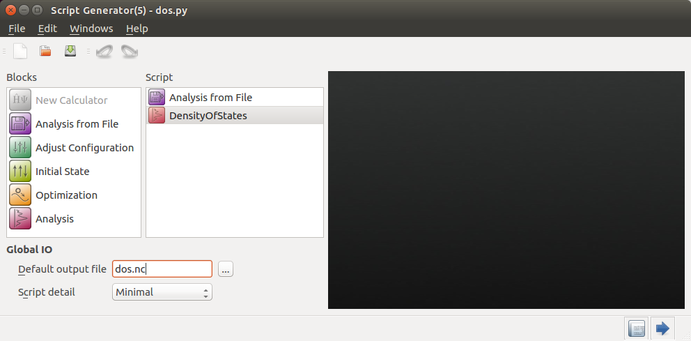
Open the Script Generator and add the  Analysis from File and
blocks. Change the default
output file to
Analysis from File and
blocks. Change the default
output file to dos.nc.
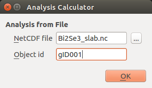
Open the first block, and point to the Bi2Se3_slab.nc file and
Object id glD001, which is the self-consistent SOGGA state.
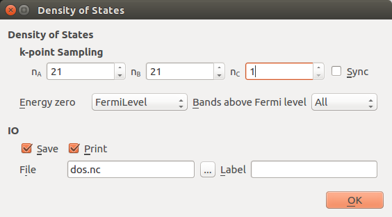
Then open the DensityOfStates analysis block, and set up a dense k-point sampling along kx and ky, 21x21x1. You will need to uncheck the sync option. Remember: It is important in this case to sample the \(\Gamma\)-point, so we use use an odd k-grid.
Save the script as dos.py and run it. You can also download it
here: dos.py.
Then locate the DOS object on the LabFloor, and use the 2D Plot plugin to visualize it. With a bit of zooming you should be able to see the expected linear dependence of the DOS on energy, as illustrated below. The sharp increase in DOS at E=0.47 eV are due to the lowest bulk conduction bands.
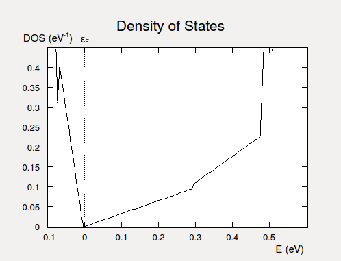
Fig. 41 Electronic DOS for the Bi2Se3 slab. Due to the Dirac cone, the DOS depends linearly on the energy in the vicinity of the Fermi level.
Penetration depth of surface states
An essential feature of the topologically protected surface states close to the Dirac point is that they are highly localized to the surface region. The penetration depth into the bulk material may be as small as 2–3 nm [4]. Moreover, the degenerate surface states observed in a band structure calculation are in each specific k-point composed of states with opposite spin and localized on opposite sides of the slab.
You will now investigate this by performing a BlochState analysis in a specific k-point on the Dirac cone for bands 144 and 145. You will then project both Bloch states onto the C-axis of the Bi2Se3 slab unit cell, and plot the magnitude and direction of the non-collinear spin vectors as a function of the C-coordinate.
Calculations
You will need the following two scripts: bloch_states.py and spinVector.py.
Download the scripts and execute the first one (bloch_states.py)
using the Job Manager or in a Terminal. It reads in the SOGGA state from
Bi2Se3_slab.nc, performs the two BlochState analyses for k-point
[0, 0.04, 0], and then computes the length \(r\) and polar angles
\(\theta\) and \(\phi\) for both Bloch states and plots them.
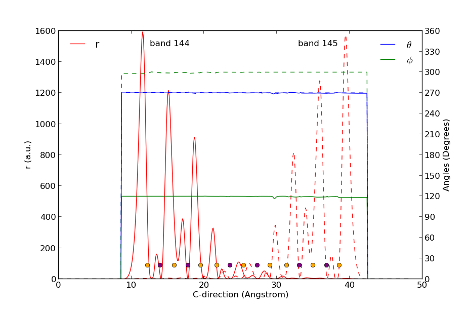
Fig. 42 Surface Bloch states in bands 144 and 145 evaluated in k-point [0, 0.04, 0]. The states are projected onto the C-direction. The states are localized on opposite sides of the slab configuration, and their spin directions are opposite.
The resulting figure is shown above. Orange and purple dots at the bottom indicate the position of the Se and Bi atoms, respectively. The two states are clearly localized on opposite sides of the slab (red curves) and have very little overlap in the middle of it. The polar angle \(\phi\) is 270° for both states (blue curves), but the in-plane angle \(\phi\) is 120° for band 144 and rotated by 180° to 300° for band 145 (green curves). The two spin states therefore point in opposite directions!
Fermi surface and spin directions
Finally, it is interesting to study the Fermi surface of the Bi2Se3 slab in the vicinity of the Dirac cone. This is easily done by sampling the band structure on a dense k-grid centered at the \(\Gamma\)-point.
Download and execute this pre-made script: fermi_surface.py. It reads
in the SOGGA state from Bi2Se3_slab.nc, performs band structure
analysis in all points on a
kx \(\times\) ky=51\(\times\)51 grid,
and creates a contour plot of the eigen-energies of the surface state
in energy band 144.
Note
For users of QuantumATK 2017: Use instead the script fermi_surface_2017.py.
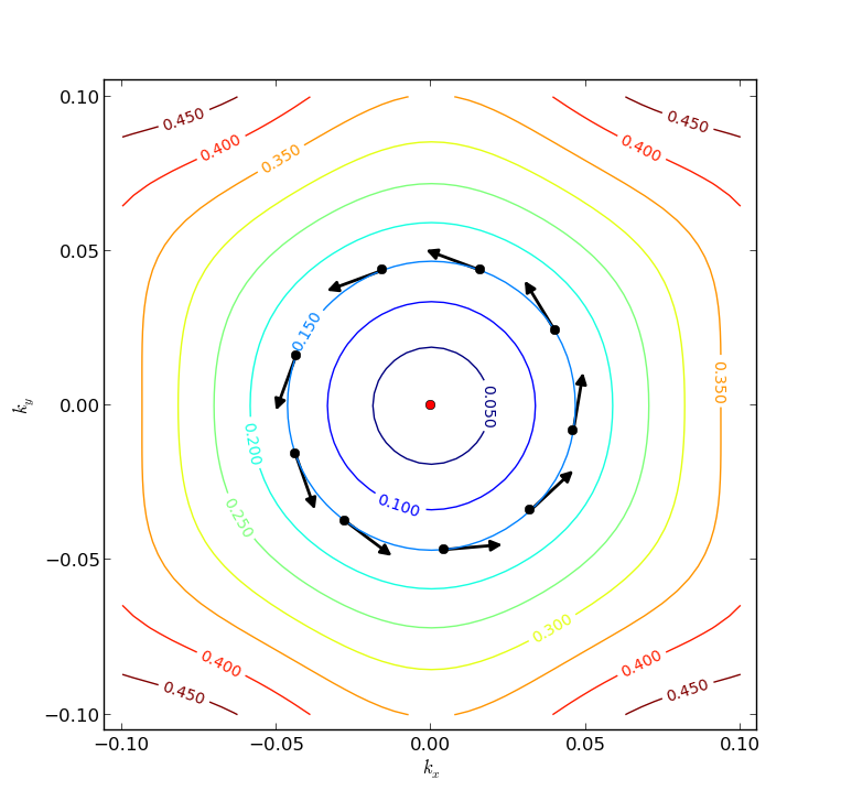
Fig. 43 Fermi surfaces on the Dirac cone centered at the \(\Gamma\)-point. The arrows indicate how the in-plane spin direction varies as an electron circles around the Dirac point.
The resulting plot is illustrated above. As expected for a Dirac cone, the Fermi surface is circular close to the apex (red dot), but in this case it turns more hexagonal in shape for higher energies.
The Python script has also extracted the contour corresponding to EF=0.15 eV and computed the Bloch state for every 10th (kx, ky) point around that contour. In each point, an arrow indicates the in-plane spin orientation (\(\phi\)). It is clear that the spin rotates by \(2 \pi\) as it circles around the Dirac point.
The reason for this is simple: Time-reversal symmetry requires that states at momenta k and -k have opposite spin. However, the Dirac cone for surface states originating from a single surface is not spin degenerate. The spin must therefore rotate with k as it goes around the Fermi surface. See Ref. [1] for more details.
Topological Invariants
The properties of a 3-D topological insulator is determined by four topological invariants [5], [6], [7], which describe properties of the band structure at special k-points, i.e. the \(\Gamma\)-point and the Brillouin zone edges.
The first topological invariant describes the difference in the wavefunction symmetry at the different special k-points. This invariant distiguishes “strong” topological insulators, and when present, the system will have topologically protected surface bands. The topological invariant is robust towards atomic disorder and any time-invariant perturbation cannot remove the surface bands.
For a system with inversion symmetry the topological invariants can be calculated from the symmetry of the Bloch function at 8 special Brillouin zone points [8],
where \({\bf b_i}\) are the reciprocal lattice vectors and \(n_i=0,1\).
Let \(\psi_{i, n}\) be the nth occupied Bloch function at \(\Gamma_{i}\), then we define the symmetry function
where \(\Theta\) is the inversion operator. Once the symmetry functions are known the strong topological invariant, \(\nu_0\), is given by
There are three weak invariants, \(\nu_1\), \(\nu_2\), and \(\nu_3\), given by products of four \(\delta_i\)‘s, for which \(\Gamma_{i}\) reside in the same plane:
The weak invariants are not robust towards atomic disorder, and do not guarantee the existence of metallic surface bands.
Python script for the calculating the topological invariants
Download the script TopologicalInvariant3D.py, which implements
the equations given above for calculating the topological invariants.
The script will only work for systems with inversion symmetry. An
example of usage is given with the python script below.
from TopologicalInvariant3D import topologicalInvariant3D

bulk_configuration = nlread('Bi2Se3_bulk.nc', BulkConfiguration)[-1]

print '-----------------------------------'
print 'Topological Invariants = ', topologicalInvariant3D(bulk_configuration)
print '-----------------------------------'
which when run will produce the output
-----------------------------------
Topological Invariants =  [1 0 0 0]
-----------------------------------
We see that Bi2Se3 is a strong 3D topological insulator, because \(\nu_0=1\), while the three weak invariants are all 0.
You can now easily screen a range of 3D materials with inversion symmetry for their topological indices to figure out if they are strong or weak topological insulators.
Note
For users of QuantumATK 2017 and later: The script TopologicalInvariant3D.py
will not work with QuantumATK 2017 and later versions. Download instead
the script TopologicalInvariant3DATK2017.py and use it like this:
from TopologicalInvariant3DATK2017 import topologicalInvariant3D

bulk_configuration = nlread('Bi2Se3_bulk.nc', BulkConfiguration)[-1]

print '-----------------------------------'
print 'Topological Invariants = ', topologicalInvariant3D(bulk_configuration)
print '-----------------------------------'