Relaxation of devices using the OptimizeDeviceConfiguration study object
Version: O-2018.06
This tutorial introduces you to the OptimizeDeviceConfiguration study object.
For proper optimization of the geometry of a 2-probe device configuration,
we recommend the Bulk Rigid Relaxation (BRR) method.
However, this can be a complicated task involving
several steps. As shown in this tutorial, the OptimizeDeviceConfiguration
study object automates the BRR method,
making it very simple to optimize the geometry of a device.
Note
The OptimizeDeviceConfiguration study object was introduced in the O-2018.06 release, and is the recommended way of performing device geometry optimizations in QuantumATK. Users of previous versions can still perform the calculations in a more complex, and manual, workflow, as described here: Advanced device relaxation - manual workflow

Introduction
In principle, the complex device structural relaxation can be done manually,
as described in the Advanced device relaxation - manual workflow tutorial, but the manual
BRR procedure requires tedious and time-consuming work. Therefore, we encourage
you to use the OptimizeDeviceConfiguration study object for relaxing
complex device systems. The study object allows for fully automated device
relaxation, including automatic identification of the central region atoms
that should be allowed to relax. This fully automated procedure is illustrated
below, and can be described as follows:
1. The region of full relaxation is determined. This happens automatically by first determining which parts of the central region are periodic repetitions of the near-by electrode. The middle point between left and right periodic images is then the center of the region that should be fully optimized, and the region has a user-specified width. Note that the region of full relaxation is not allowed to extend into an electrode extension. If it does, the edge of the region is automatically moved to the border of that electrode extension.
2+3. Bulk Rigid Relaxation is executed. The device configuration is converted to a bulk configuration (the electrodes are removed), and the right-hand end of the cell is extended with a vacuum region, in order to allow for contraction or expansion of the central region during relaxation. Ordinary geometry optimization (force minimization) is then executed while applying a Fixed constraint on the left-hand atoms and a Rigid constraint on the right-hand atoms. See the tutorial Advanced device relaxation - manual workflow for more details on the BRR method.
4. The device configuration is re-assembled. The vacuum region is removed and the electrodes are attached, resulting in the final geometry optimized device configuration.
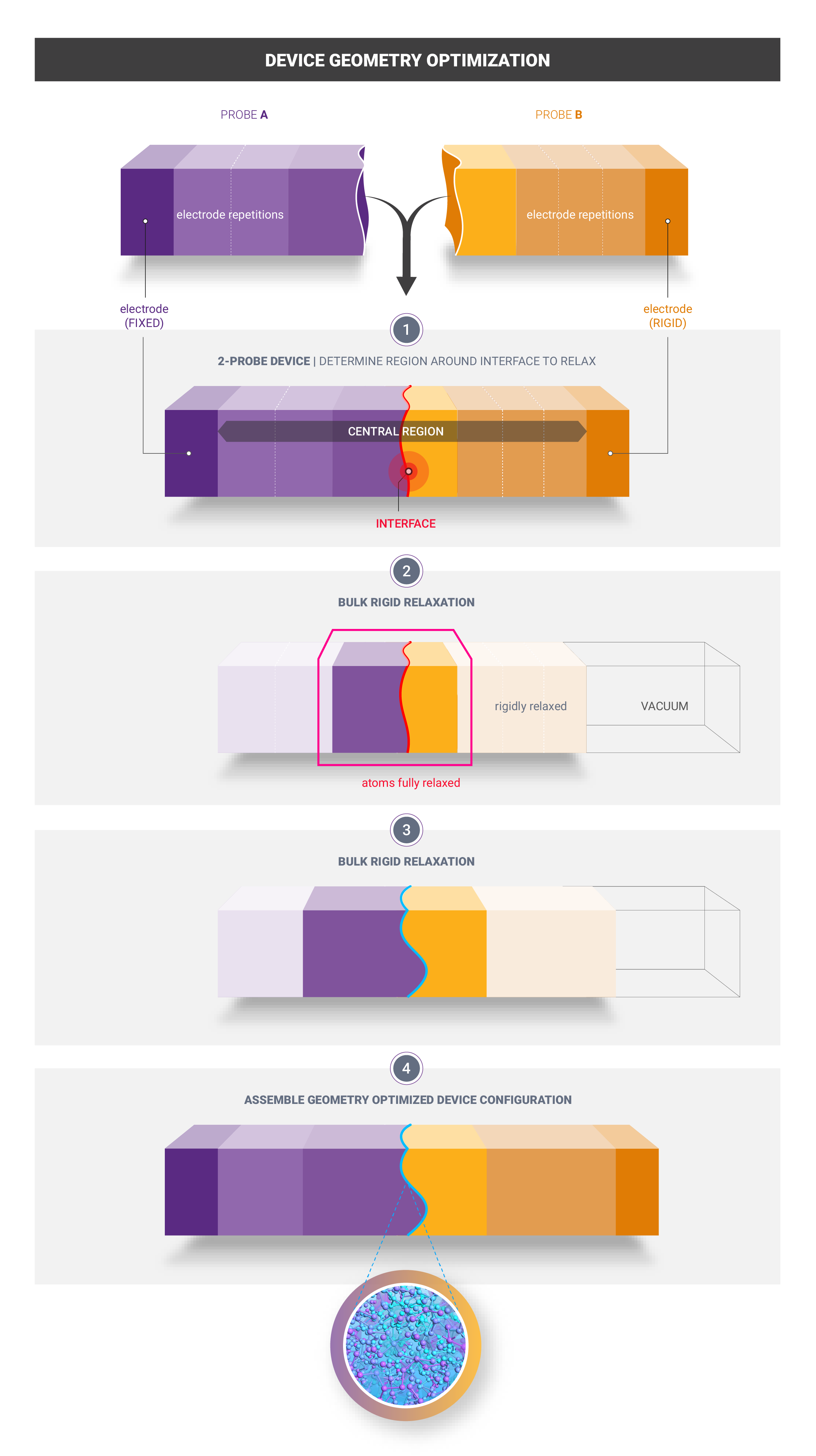
The study object allows you to change certain settings for device relaxation:
You may select which part of the central region to fully relax, i.e., you may specify the center and width of the relaxation region.
The relaxation region may extend to the entire device, except of course the electrodes and their extensions.
If needed, the left and right surfaces of the central region may be hydrogen-passiovated during steps 2 and 3.
The usual force convergence criterion for gemoetry optimization may also be tuned.
We will here demonstrate how geometry optimization of a Ag(100)||Au(111) interface
can be done using the  OptimizeDeviceConfiguration study object.
For purposes of illustration, a large defect is introduced at the Ag|Au interface
in order to enhance the effect of geometry optimization.
OptimizeDeviceConfiguration study object.
For purposes of illustration, a large defect is introduced at the Ag|Au interface
in order to enhance the effect of geometry optimization.
Unrelaxed Ag(100)|Ag(111) device
The unrelaxed and defected Ag(100)|Ag(111) device is available as a script: unrelaxed.py.
Please download it and use it for this tutorial.
The device was built using the Interface Builder,
as shown in the tutorial Building an interface between Ag(100) and Au(111).
The defect at the Ag|Au interface was introduced by simply removing atoms
using the  Builder.

Important
In general, devices should be built from relaxed (unstrained) materials, i.e., the electrodes should be in equilibrium geometries (given the level of theory employed, for example DFT using the PBE exchange-correlation functional, or a particular force field).
This may be crucial, as the theoretically predicted electronic properties of a material will in general depend on the geometry. In particular, the electrode relaxation may have an effect on the band gap and effective masses of the electrode material, which may change IV characteristics of the device. An instructive example of relaxation for strained silicon electrodes is given in Appendix.
The OptimizeDeviceConfiguration study object does not relax the
electrodes – it is the responsibility of you as a user to make sure
the electrode geometries are appropriate before running the device
geometry optimization.
Set up and run the device geometry optimization
Send the script unrelaxed.py to the  Script Generator.
You will here relax the device using the ATK-ForceField engine,
in order to speed up calculations.
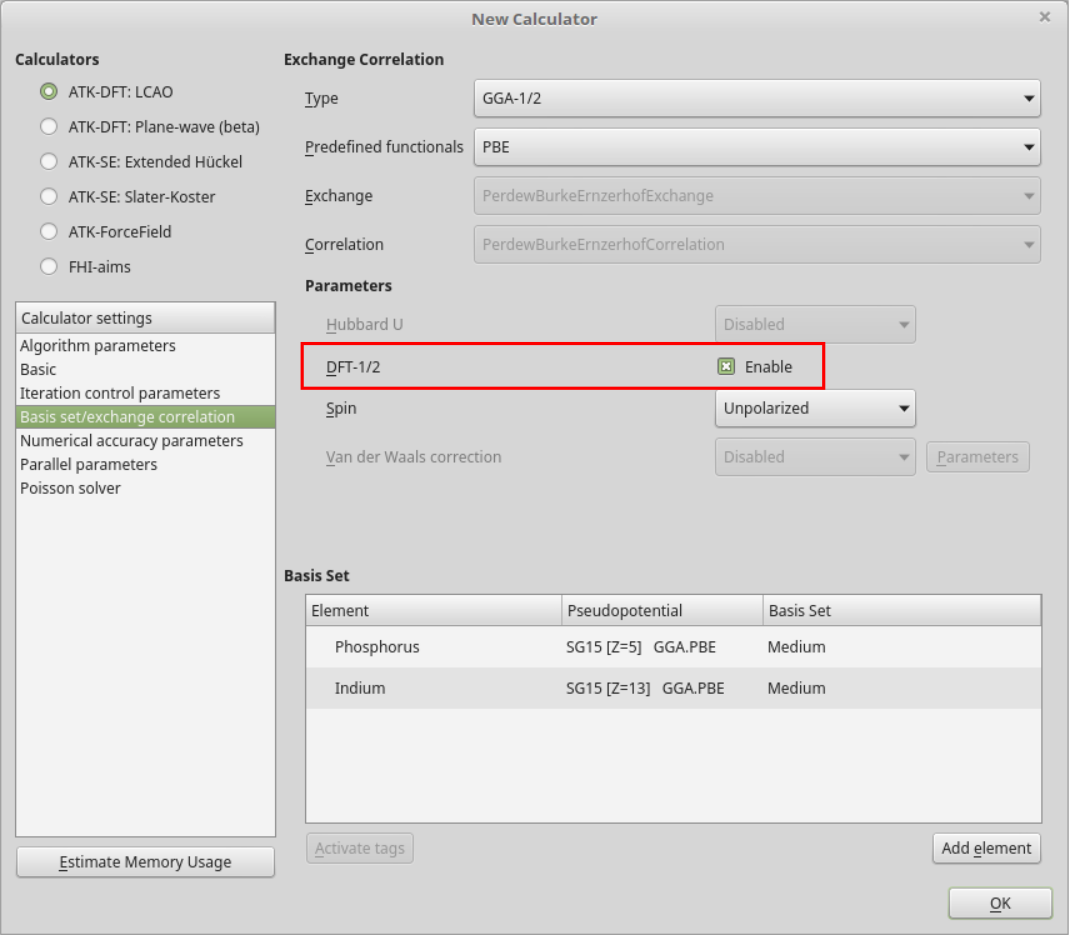
In the Script Generator, add the  New Calculator
block, and double-click to open it. Then select the ATK-ForceField calculator
and choose the EAM_Zhou_2004 force field.
New Calculator
block, and double-click to open it. Then select the ATK-ForceField calculator
and choose the EAM_Zhou_2004 force field.
Next, add the OptimizeDeviceConfiguration study object script block,
by clicking .
We will run the device geometry optimization using both A) default settings, and B) a custom optimization region.
A) Default settings
Double-click the OptimizeDeviceConfiguration block to open it. In principle, none of the settings need to be changed. As you see below, the default width of the optimization region is 10 Å, and the option Optimization region center is unticked, so the center is automatically determined, as described above.
Leave the settings at default values, close the widget, and change the
name of the output results file to Ag100-Au111-default.hdf5,
and save the Python script as Ag100-Au111-default.py.
You may also download the final script: Ag100-Au111-default.py.

Note
The options Passivate left electrode and Passivate rigth electrode
are ticked by default, meaning that the OptimizeDeviceConfiguration
study object will attempt to apply hydrogen passivation to the
left and right surfaces during the central region bulk relaxation
(steps 2+3 in the methodology outlined in the Introduction).
This can be of relevance for semiconducting materials, but has no impact on metallic systems such as the Ag(100)|Au(111) interface.
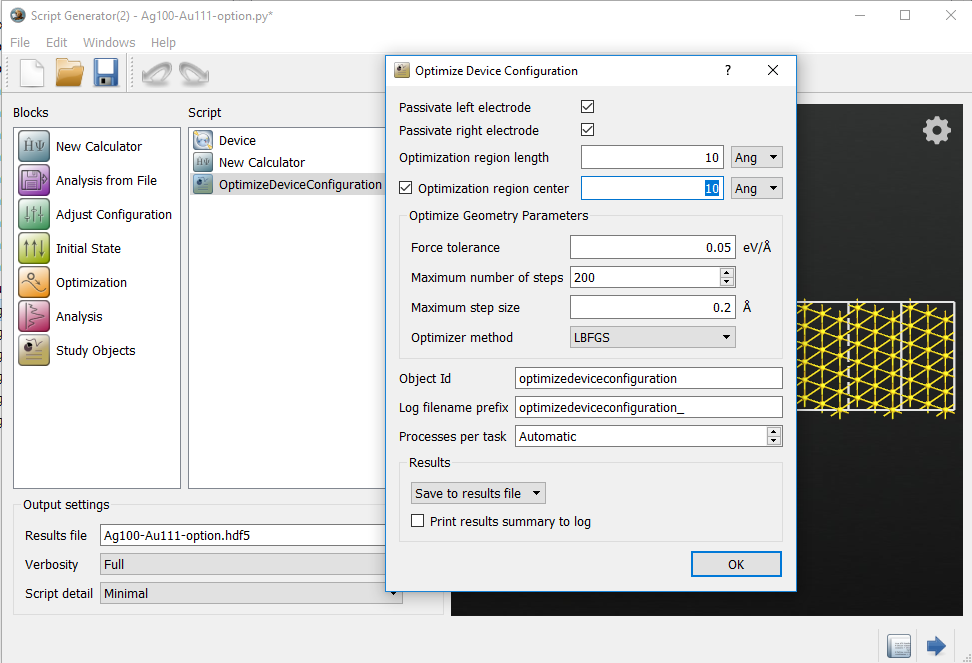
B) Custom optimization region
Open again the Optimize Device Configuration widget. For demonstration purposes, you will now specify an optimization region that does not include the Ag|Au interface. The atoms around the interface will therefore not be relaxed.
Tick the option Optimization region center, and set the center position to 10 Å, which is measured from the right-hand edge of the left-hand electrode. Keep the optimization region length at 10 Å, such that only atoms within \(\pm\)5 Å from the center will be allowed to relax.
Note that, since the left electrode extension is of 8.17 Å, i.e., larger than 5 Å, the specified optimization region extends into the electrode extension. This overlap region will not be relaxed because the NEGF method requires that the electrode extension is identical to the electrode.
Finally, close the widget, and change the name of the output results file to
Ag100-Au111-option.hdf5, and save the Python script as Ag100-Au111-option.py.
You may also download the final script: Ag100-Au111-option.py.
Run the calculations
Run the two ATK Python scripts, either using the  Job Manager
or from a terminal:
Job Manager
or from a terminal:
atkpython Ag100-Au111-default.py > Ag100-Au111-default.log
The device geometry optimizations will take only a few seconds to execute.
Relaxed device structures
The NanoLab LabFloor should now show the contents of the two saved HDF5 output
data files. If not, tick the output files in the left-hand Project Files list.
Each file contains the OptimizeDeviceConfiguration object
and the optimized DeviceConfiguration.
Use the  Viewer to inspect the optimized devices. You may send
the unrelaxed device configuration from the Builder to the Viewer
for easy comparison.
Viewer to inspect the optimized devices. You may send
the unrelaxed device configuration from the Builder to the Viewer
for easy comparison.
The figure below compares device configurations before and after geometry optimization
for case A (default settings, Ag100-Au111-default.hdf5).
You can clearly see the effect of structural relaxation. The periodic repetitions
of the left and right electrodes are also indicated, as well as the 10 Å
wide region of full atomic relaxation.

The next figure compares the optimized devices from case A (default settings) and case B (custom optimization region). It is clear that we in case B made a very poor choice of optimization region: Very little relaxation has happened, and the region around the Ag|Au interface is completely unrelaxed. There are two reasons for this:
The optimization region center is set too close to the left electrode;
The optimization region length does not cover the interface region with the defects.

The Text Representation gives information about the settings used for the OptimizeDeviceConfiguration study object, and a summary of the results. To use it, select one or more OptimizeDeviceConfiguration objects on the LabFloor, and click the Text Representation tool in the right-hand plugins bar.
The text representation reports for case A (Item: 0) and case B (Item: 1)
are shown below.
# Item:  0
# File:  C:\ATK\OptimizeDeviceConfiguration\Ag100-Au111-default.hdf5
# Title: Ag100-Au111-default.hdf5 - optimizedeviceconfiguration
# Type:  OptimizeDeviceConfiguration
+------------------------------------------------------------------------------+
| Optimize Device Configuration Report                                         |
+------------------------------------------------------------------------------+
| Device configuration:                                                        |
+------------------------------------------------------------------------------+
| Central region (including electrode extensions):                             |
|     Length (before optimization): 54.97 Ang                                  |
|     Length (after optimization): 54.67 Ang                                   |
|     Number of atoms: 135                                                     |
| Electrode extensions:                                                        |
|     Length (left): 8.17 Ang                                                  |
|     Length (right): 7.06 Ang                                                 |
|     Number of atoms (left): 20                                               |
|     Number of atoms (right): 18                                              |
+------------------------------------------------------------------------------+
| Optimization details:                                                        |
+------------------------------------------------------------------------------+
| Optimization region:                                                         |
|     Length: 10.00 Ang                                                        |
|     Left edge position: 24.15 Ang                                            |
|     Right edge position: 34.15 Ang                                           |
|     Number of atoms: 21                                                      |
| Constrained regions:                                                         |
|     Length (left): 24.15 Ang                                                 |
|     Length (right): 20.82 Ang                                                |
|     Number of atoms (left): 60                                               |
|     Number of atoms (right): 54                                              |
+------------------------------------------------------------------------------+

# Item:  1
# File:  C:\ATK\OptimizeDeviceConfiguration\Ag100-Au111-option.hdf5
# Title: Ag100-Au111-option.hdf5 - optimizedeviceconfiguration_option
# Type:  OptimizeDeviceConfiguration
+------------------------------------------------------------------------------+
| Optimize Device Configuration Report                                         |
+------------------------------------------------------------------------------+
| Device configuration:                                                        |
+------------------------------------------------------------------------------+
| Central region (including electrode extensions):                             |
|     Length (before optimization): 54.97 Ang                                  |
|     Length (after optimization): 54.97 Ang                                   |
|     Number of atoms: 135                                                     |
| Electrode extensions:                                                        |
|     Length (left): 8.17 Ang                                                  |
|     Length (right): 7.06 Ang                                                 |
|     Number of atoms (left): 20                                               |
|     Number of atoms (right): 18                                              |
+------------------------------------------------------------------------------+
| Optimization details:                                                        |
+------------------------------------------------------------------------------+
| Optimization region:                                                         |
|     Length: 6.83 Ang                                                         |
|     Left edge position: 8.17 Ang                                             |
|     Right edge position: 15.00 Ang                                           |
|     Number of atoms: 15                                                      |
| Constrained regions:                                                         |
|     Length (left): 8.17 Ang                                                  |
|     Length (right): 39.97 Ang                                                |
|     Number of atoms (left): 20                                               |
|     Number of atoms (right): 100                                             |
+------------------------------------------------------------------------------+
Item 0
For case A, you can see the following information in the text representation:
The central region includes 135 atoms, and initially had a length of 54.97 Å along the transport direction, which decreased slightly to 54.67 Å during relaxation.
The length of the left (right) electrode extensions are 8.17 Å (7.06 Å), containing 20 (18) atoms each.
The optimization region length is 10 Å, and the position of the left (right) optimization region edge is at 24.15 Å (34.15 Å), leading to 21 fully relaxed atoms.
The left and right parts of the device that are constrained during relaxation are 24.15 Å and 20.82 Å long, respectively, and contain 60 and 54 atoms.
Item 1
For case B, we observe that
The length of the optimization region is only 6.83 Å, because it has been automatically reduced in order to avoid relaxing the electrode extension.
The right-hand edge of the optimization region is at 15 Å, so the Ag|Au interface is not relaxed.
Full atomic relaxation has therefore only been done in a region comprising bulk-like Ag, so very little relaxation has actually happened. This is also indicated by that fact that the central region length did not change at all during geometry optimization.
Conclusions
When using the OptimizeDeviceConfiguration study object, you may
take full control of what is to be the region of full atomic relaxation,
by manually setting the center and width of this region.
However, it is important to carefully check the result.
Alternatively, you may choose to let the relaxation region extend over the full device, or simply stick to the default 10 Å width and automatic detection of the region center.
In summary, there are three main modes of operation for the
OptimizeDeviceConfiguration study object:
Use default optimization region settings (10 Å width and automatic detection of the region center).
Manually specify the optimization region center and width.
Relax all central region atoms (except the electrode extensions) by increasing the optimization region width beyond the central region total length.
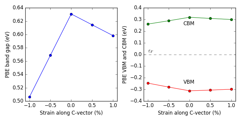
Appendix
As previously mentioned, devices should in general be built from relaxed materials, to avoid effects of stress or strain on the electronic properties. If the starting materials are not relaxed before building the device, geometry optimization of the device may compensate for this by artificially straining parts of the device along the transport direction.
We here show one example of the effect strain on the electronic structure of a semiconductor electrode. The below figure shows the band structure of a Si(100) electrode strained by \(\pm\)1% along the C-axis, which coincides with the (100) crystallographic direction. By careful inspection one can see that the conduction and valence band energies get slightly shifted.
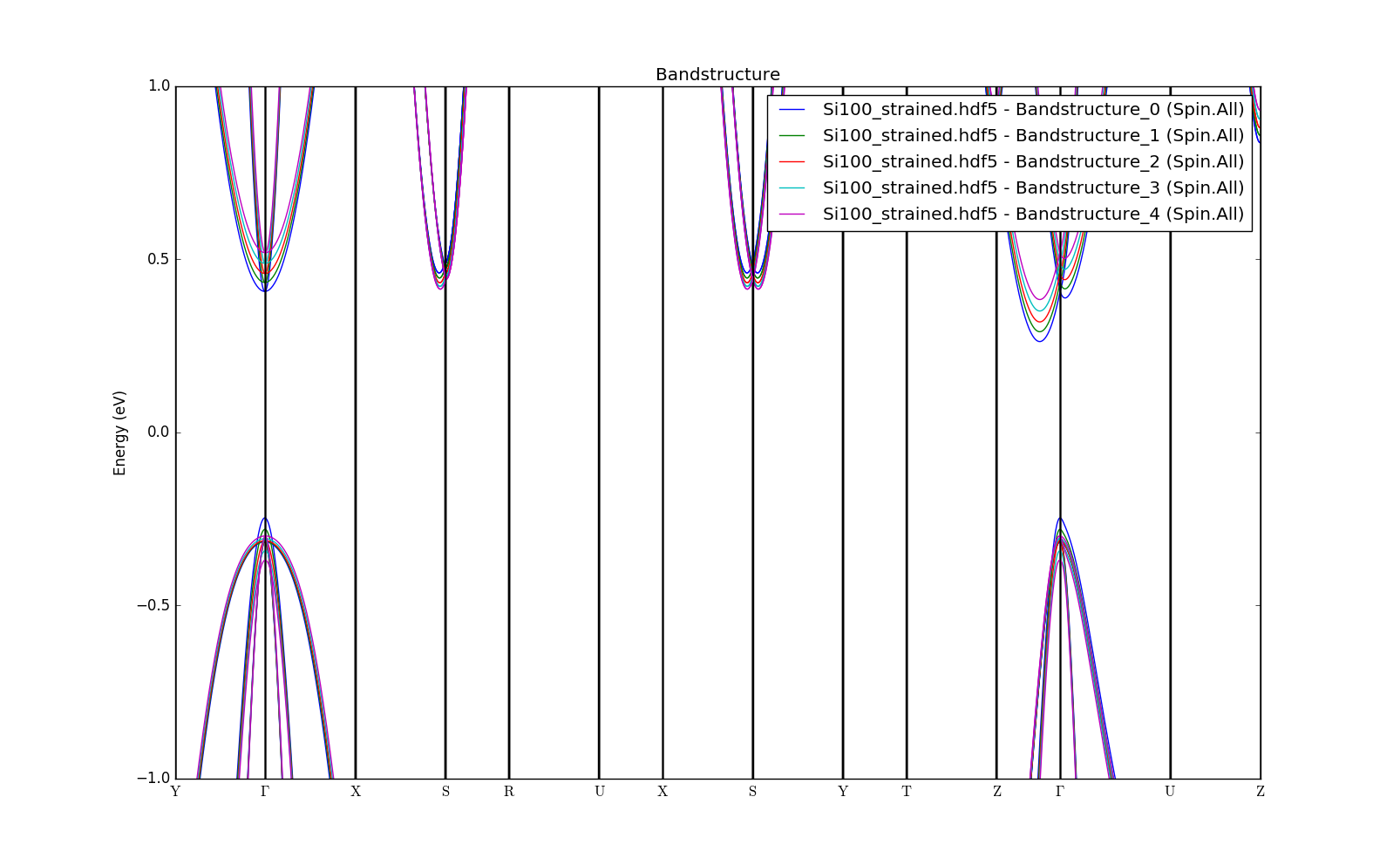
The figure below shows how the DFT-PBE valence band maximum (VBM) and conduction band minimum (CBM) change upon straining the Si(100) electrode along the C-axis (right-hand panel), and how the silicon fundamental band gap therefore also changes (left-hand panel).