In this tutorial you will learn about two topics: (i) bandstructure
calculations by density functional theory (DFT) with the meta-generalized-
gradient approximation (meta-GGA) exchange-correlation (XC) functional of Tran & Blaha (TB09)
and (ii) calculations of confined structures with focusing on how to
passivate dangling bonds on the surface. After completing the tutorial,
you will be able to:
Perform calculations with the TB09 meta-GGA XC functional to obtain accurate band gaps of semiconductors;
Set up and passivate confined III-V systems (InAs, GaAs, InP, …);
Use special pseudopotentials with non-integer charges for the
passivating hydrogens, that is, artificial hydrogen atoms or
pseudo-hydrogens, which are needed in order to passivate III-V and
II-VI surfaces since normal hydrogen passivation leads to metallic
surface states;
Use compensation charges on the passivating (normal) hydrogen atoms as
an alternative to using pseudo-hydrogens.
Note
If you are not yet familiar with QuantumATK, go through the basic
tutorials first. The underlying calculation
engines for this tutorial is ATK-DFT, about which one can find the details
in QuantumATK Reference Manual.
DFT is infamous for predicting too small band gaps, when calculated from the
Kohn-Sham energy eigenvalues. However, recent advances of meta-GGA
functionals have enabled us to compute accurate band gaps.
Meta-GGA functionals belong to the third rung of the so-called Jacob’s
ladder of XC functionals, as they not only include the local density
\(\rho(\mathbf{r})\) (as in LDA; the first rung) and the gradient of the
density \(\nabla\rho(\mathbf{r})\) (as in GGA; the second rung), but
also the kinetic-energy density \(\tau(\mathbf{r})\). In 2009, Tran and
Blaha [1] showed that accurate band gaps could be obtained for a broad
range of materials. In their formulation, the exchange potential is given by
where \(\tau(\mathbf{r})=1/2\sum_{i=1}^N|\nabla\psi_i(\mathbf{r})|^2\)
is the kinetic-energy density, \(\psi_i(\mathbf{r})\) is the i’th
Kohn-Sham orbital, and \(v_x^{BR}(\mathbf{r})\) is the Becke-Roussel
exchange potential [2]. The parameter c is calculated as
where \(\alpha=-0.012\) and \(\beta=1.023\ \mathrm{Bohr}^{1/2}\)
were determined by fitting to reproduce the experimental band gaps of a
large number of semiconductors and insulators and \({\Omega}\) is the
volume of the cell. The correlation potential used by Tran and Blaha is an ordinary LDA correlation.
In ATK you can use the XC functional by Tran and Blaha in two ways. You can specify the XC functional as
exchange_correlation=MGGA.TB09LDA
in which case the c-parameter is determined self-consistently based on the
expression above. This is the default, and the way the script is set up by Script Generator in QuantumATK.
You can also set the value of the c-parameter manually:
exchange_correlation=MGGA.TB09LDA(c=1.0)
The electron and kinetic-energy densities are still calculated fully
self-consistently, but using the fixed value of c.
If the c-parameter is calculated self-consistently, the value will be
printed in the log file. It can also be extracted in a script as
c=calculateTB09C(bulk_configuration)
after the self-consistent calculation.
Note
Using a self-consistent determination of the c-parameter should only be done for a bulk configuration that is periodic in all directions. A confined system such as a slab or a nanowire will include large regions of vacuum. Since the c-parameter is calculated as an integral over the whole unit cell volume, the contributions from the vacuum region will lead to incorrect, even diverging results. You will most likely see warning messages in the log file if you attempt this .
For confined systems one must first determine an appropriate value for c for the corresponding bulk system. This can be done either self-consistently or by fitting the c-parameter to, e.g., the experimental band gap (see Fitting the TB09 meta-GGA c-parameter). The so-determined c-parameter can then be used for the confined structure.
You should now setup an InAs bulk crystal. In Builder,
click Add‣Database…,
type InAs in the search field, and add the structure to the Stash.
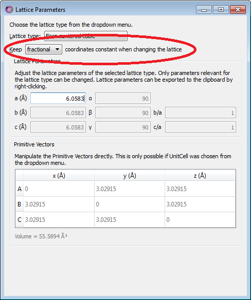
The next step is to change the lattice constant to the experimental room temperature lattice constant, \(a=6.0583 Å\)[3]
In the panel to the right, open Bulk tools‣Lattice Parameters…
Importantly, you must select to keep fractional coordinates constant (see the figure below), else the symmetry of the crystal will be broken when the lattice constant is changed.
In the following you will calculate the band structure of bulk InAs using the TB09 meta-GGA functional with the c-parameter calculated self-consistently and non-self-consistently.
For this purpose:
Add New Calculator and Bandstructure blocks.
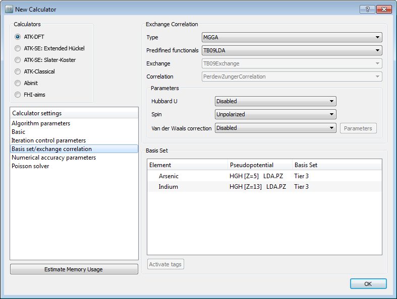
Open the New Calculator block, and make the following changes:
Set Exchange correlation to meta-GGA
Set the k-point sampling to 7, 7, 7.
Under Basis set/exchange correlation, change the pseudopotentials to “HGH[Z=5], LDA.PZ” for Arsenic and “HGH[Z=13], LDA.PZ” for Indium. Choose the Tier 3 basis set for both elements.
Finally set the output filename to InAs_hgh.nc.
Save the script, then send it to Job Manager,
by using the “Send To” icon, and run the job. The calculation will take just a minute or two.
Note
For self-consistent calculations of the c-parameter, more accurate band structures
are usually obtained using the HGH pseudopotentials which include semi-core states.
This is the case for HGH[Z=13] above for Indium, which include the ten 4d electrons,
in contrast to HGH[Z=3] which only includes the 3 valence electrons (5s and 5p states).
Semi-core pseudopotentials are however only provided in ATK for some elements; for Arsenic
there is only a HGH[Z=5] pseudopotential, without pseudocore states.
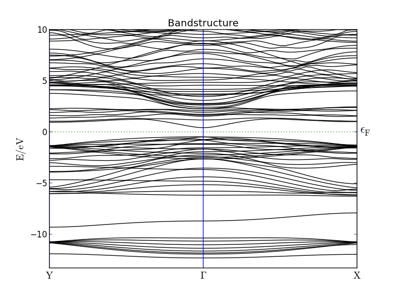
Band structure for self-consistently determined c
When the calculation finishes, locate the band structure object on the LabFloor and click Bandstructure Analyzer to plot the band structure like below.
You will find that the calculated band gap is very close to the experimental value 0.354 eV. This is actually a quite general trend, when using the HGH pseudopotentials.
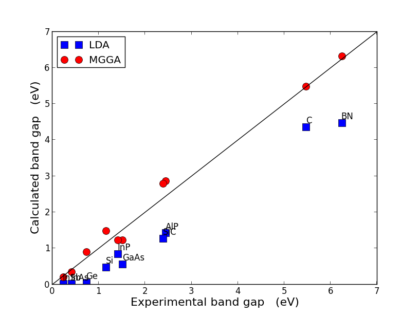
The figure below shows the calculated vs. experimental band gaps for a range of semiconductors and insulators. Results are shown for both LDA and TB09 meta-GGA calculations
(additional examples are provided in Ref. [1]) and show that while LDA always underestimates the band gaps (the famous band gap problem in DFT),
the TB09 meta-GGA results are generally quite close to the experimental values, and typically as accurate as the results of much more expensive hybrid functional or even GW calculations.
Fig. 96 Calculated vs. experimental band gaps. The calculations are performed with
LDA (blue squares) and TB09 meta-GGA (red circles) XC functionals.
For the TB09 meta-GGA calculations, the HGH pseudopotential have been used with a Tier 4 basis set,
and the c-parameter is calculated self-consistently.
While HGH pseudopotentials in general gives rather accurate band gaps by computing the c-parameter self-consistently, it might be desirable to
get an even closer agreement with experimental values. In order to achieve that, it is possible to manually set the TB09 meta-GGA c-parameter such that
the calculated band gap coincides with the experimental one. This can also be used as a way to compensate for a slightly less accurate pseudopotential or basis set, as will be illustrated in this section.
Go back to Script Generator and open the New Calculator block, and make the following settings:
Under :menuselection:Basis set‣exchange correlation, change the pseudopotentials to “FHI[Z=5], LDA.PZ” for Arsenic and “FHI[Z=3], LDA.PZ” for Indium. That is, choose pseudopotentials without semicore states.
Set the basis set to DoubleZetaPolarized for both elements.
Change the output filename to “InAs_c_fit.nc”
Send the script to Editor, by using the “Send To” icon.
In Editor, go to the line where the XC function is specified and add the c-parameter argument to the MGGA.TB09LDA functional.
Then send the script to Job Manager (again use the “Send To” icon) and run the calculation. This time it will only take a few seconds.
When the calculation is done, plot the band structure and measure the band gap.
If the the gap is larger than the experimental value (0.354 eV), then go back to
Editor and decrease the c-value a bit and run again. If the band gap is smaller,
you must increase the c-value. Try a few iterations to see if you can get a close
agreement with the experimental value.
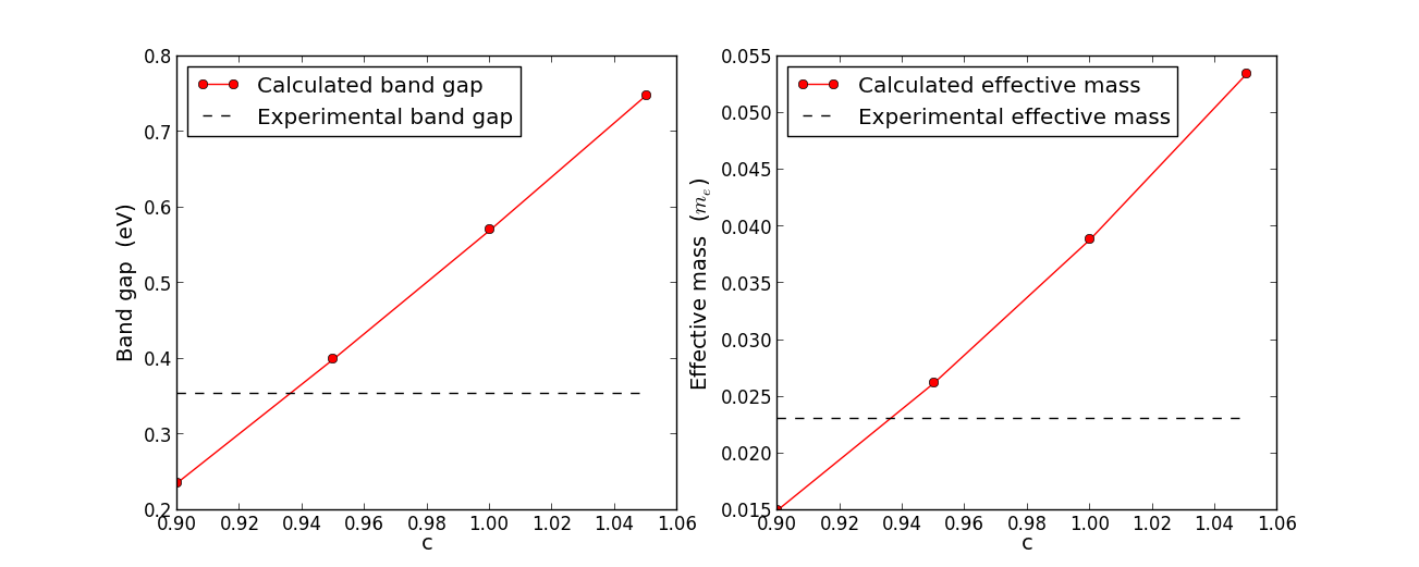
The figures below show the calculated band gap (left panel) for four different
c-values (0.9, 0.95, 1.0, 1.05). Due to the very linear behavior, we can
safely find the optimal c-parameter at the intersect between the interpolated line of the calculated
band gaps and the experimental gap. This yields an optimal c-value of 0.936,
which we will use in the following.
The right panel shows the calculated conduction band effective mass for the same
four c-values. Also indicated is the experimental conduction band mass (0.023 \(m_e\)).
The lines cross at c=0.935, so - very importantly - approximately the same c-value optimizes both
the band gap and the effective mass, thus giving a very good description at least of the
lowest \(\Gamma\) valley of InAs.
Fig. 97 Calculated band gap (left) and conduction band effective mass (right) vs.
the TB09 meta-GGA c-parameter. Increasing c will always lead to a larger band gap.
Both the band gap and the effective mass are optimized by approximately the same
c-parameter (0.936).
Before continuing to study confined InAs structures, you will first calculate and analyze the bulk band structure with the optimized c-parameter in some more detail.
Go back to Script Generator and make the following adjustments:
Delete Bandstructure object.
Insert an LocalBandstructure block and open it (see figure below).
Set “Bands below Fermi level” to 0.
Set “Points per segment” to 50.
Add a second direction: 0.5, 0.5, 0
Otherwise keep the default.
Change the output file name to “InAs_bulk_c_optimized.nc”.
Transfer the script to Editor and insert the optimized c-parameter value:
Finally, send the script to Job Manager and run the calculation.
To analyze the results, use Local Bandstructure Analyzer.
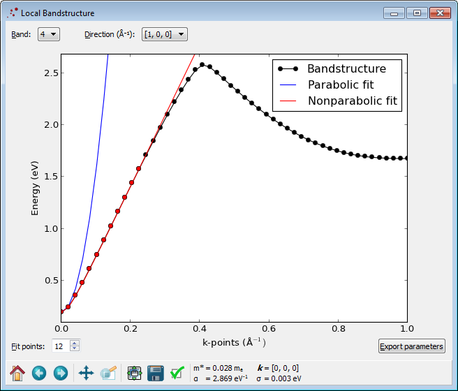
LocalBandstructure object calculates the effective mass \(m^*\) and further fits the band structure to the function \(E(1+\alpha E)=\frac{\hbar^2 k^2}{2m^*}\),
where \(\alpha\) is the parameter to fit. You can control the range of the fit with the number of Fit points. This non-parabolic dispersion relation provides a much better fit to the TB09 meta-GGA band structure than the usual parabolic model \(E=\frac{\hbar^2 k^2}{2m^*}\), as shown in the figure below. The red dots indicate the range used for fitting \(\alpha\).
Fig. 98 Local bandstructure analyzer. The black dots show the calculated band structure data, while the blue and red curves show the results of a parabolic and non-parabolic model, respectively. The fitted \(\alpha\) value is shown below the plot together with the effective mass.
From the LocalBandstructure Analyzer, we see that the InAs conduction band in the [1,0,0] direction is very accurately described by \(m^*=0.028\,m_e\) and \(\alpha=2.869\,eV^{-1}\),
while the parabolic model only describes the band well in the vicinity of the conduction band minimum.
Try to change the Direction to \((0.5, 0.5, 0)\,Å^{-1}\) to calculate the local band structure for this direction. Note that the effective mass is the same as before, i.e. it is isotropic, while the non-parabolicity parameter \(\alpha\) is not isotropic.
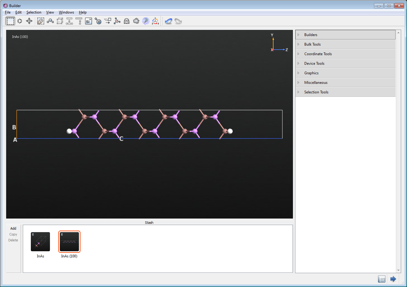
You will now setup an InAs slab which is confined in the [100] direction.
Go back to the Builder window, where it will be assumed that you still have the bulk InAs crystal from previous.
Next, Builders‣Surface (Cleave)… to cleave the crystal along the (100) direction.
Keep the default (100) Miller indices, and press “Next”.
Keep the default surface lattice vectors, and press “Next”.
Keep the default supercell - this will ensure that the wire direction is perpendicular to the surface.
Finalize your configuration by choosing “Non-periodic and normal (Slab)” configuration with a thickness of 8 layers and a top and bottom vacuum of 5 Å.
Press “Finish” to add the cleaved structure to the Stash.
The surfaces of the so-created bare InAs slab have dangling bonds due to unpaired In and As atoms.
This will lead to metallic surface states with energies in the band gap. In order to passivate
the surfaces you will now add hydrogen atoms.
Open Coordinate Tools‣Custom Passivator.
Set Hybridization to “4 (SP3)”.
Change the bond distances to 1.3 Å (otherwise neighboring hydrogen atoms will be too close).
Press the “Passivate” button.
Note
The Custom Passivator adds tags to the added hydrogen atoms - this is essential for this tutorial, so don’t change or remove them.
You can inspect the tags by opening Select‣Tags. You will later use these tags to identify H atoms bonded to In and As, respectively,
when specifying compensation charges and using specialized pseudopotentials.
The structure should now resemble the figure below.
In the following you will calculate the band structure using default settings for the passivating hydrogen atoms. For this purpose:
Add a New Calculator.
Add Analysis/Bandstructure.
Open the New Calculator block, and set exchange correlation to meta-GGA and the k-point sampling to 7, 7, 1.
Note that the FHI pseudopotentials are selected by default.
Finally, open the Bandstructure block and set the Brillouin zone route to “Y,G,X”, and increase the points per segment to 100.
As discussed in Short introduction to TB09 meta-GGA, the self-consistent calculation of the c-parameter only works for bulk systems without vacuum regions, whereas for a slab calculation one should use a fixed value.
Therefore, send the script to Editor and specify the c-parameter you found in Band structure with optimized c-parameter to reproduce the experimental band gap for the FHI pseudopotentials:
Save the script, then send it to Job Manager (again use the “Send To” icon) and run the calculation. This time it will take a bit longer, around 5 minutes.
Note
When running the script, you may observe a warning in the log file:
################################################################################# WARNING ## ## The computed TB09 meta-GGA XC potential ## diverged in 0.01 % of the simulation volume, and was ## truncated to be in the range [-10.0000, 10.0000] Hartree ## #################################################################################
You do not need to worry about this because you have set the c-parameter
to a fixed value. If, on the other hand, you were trying to calculate it self-consistently,
the warning would be relevant. However, as explained in
Short introduction to TB09 meta-GGA, the self-consistent evaluation of the c-parameter involves an integral
over the entire calculation unit cell, including the vacuum regions,
where the TB09 meta-GGA XC potential can diverge.
For confined systems like slabs and nanowires, you therefore always need
to specify the c-parameter manually.
If you now plot the result of this calculation with the Bandstructure Analyzer you will find that there is no band gap, but instead a lot of more or less
flat bands in the region around the Fermi energy. These are due to surface states, which arise due to inadequate passivation of the surface.
In order to get rid of the surface states (or rather to push them away from the Fermi level) the hydrogen atoms need to be treated differently.
The following two sections illustrate two possible ways to eliminate the surface states, to produce a proper band structure for your InAs slab.
In the following you will calculate the band structure and effective mass using so-called pseudo-hydrogen atoms containing fractional charges. The use of pseudo-hydrogen is a
well-known procedure in the literature to passivate III-V and II-VI surfaces [4].
Return to the Script Generator window and open the New Calculator block. Make the following settings to set different basis sets for
the hydrogen atoms bonded to Indium and Arsenic, respectively:
Under Basis set/exchange correlation click the Activate tags button and check both H_As and H_In for hydrogen.
This technique, i.e. using tags, allows you to assign a different basis sets to atoms of the same element, which can be a useful trick in other situations too.
Change the pseudopotential for the H_As atoms to “FHI Fractional LDA.PZ”, and set the basis set to “DoubleZetaPolarized, Z=0.75”
Change the H_In pseudopotential to “FHI Fractional LDA.PZ”, and the basis set to “DoubleZetaPolarized, Z=1.25”
Note the following important points.
Two separate hydrogen basis sets are defined: one for hydrogens bonded to Indium
atoms, and one for those bonded to Arsenic atoms.
The basis sets use different pseudopotentials with
charge 1.25 and 0.75 electrons, respectively. (From the widget it may appear
that they use the same, but the fractional pseudopotentials are automatically
selected to match the basis set charge.)
The use of these pseudopotential charges can be understood as follows [4].
The surface of an unpassivated nanocrystal consists of dangling bonds
which will introduce band gap states. The purpose of a good passivation
is to remove these band gap states. One way to do so is to pair the unbonded
dangling bond electron with other electrons. If a surface atom has m valence electrons,
this atom will provide m/4 electrons to each of its four bonds in a tetrahedral (sp3)
crystal. To pair these m/4 electrons in each dangling bond, a passivating agent
should provide (8 − m) / 4 additional electrons. Since As has m=5, it should be
passivated with pseudo-hydrogen containing (8-5)/4=0.75 electrons.
Likewise, In has m=3 valence electrons, and should be passivated with pseudo-hydrogen
with (8-3)/4=1.25 electrons.
Both types of hydrogen atoms are still charge neutral, i.e. there are 1.25 electrons
and a core with charge 1.25, and similarly for the 0.75 case.
Add a LocalBandstructure object Analysis‣LocalBandstructure and adjust the following parameters:
Set “bands below Fermi level” to 0.
Increase “Points per segment” to 50.
Set the output file name to “InAs_slab_pseudohydrogen.nc”, and send the script to Editor and make the
usual adjustment of the c-parameter.
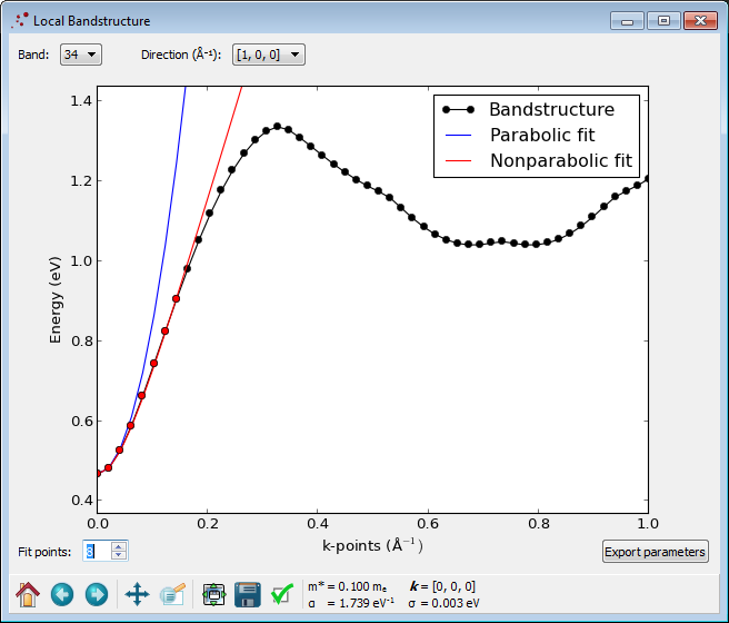
Plotting the calculated band structure with the Bandstructure Analyzer you can observe that a band gap has opened up.
The pseudo-hydrogen atoms have thus indeed moved the surface states away from the Fermi energy, as intended.
By inspecting the band structure, you can see that the band gap has increased to a value of 0.1 eV, compared to the bulk value 0.354 eV, as a result of quantum confinement.
Next you may inspect the calculated effective mass and non-parabolicity parameter using the Local Bandstructure Analyzer.
Notice that the effective mass is increased to \(0.1\,m_e\) compared to the bulk value (0.028), while the non-parabolicity parameter \(\alpha\) has decreased to 1.739 (bulk value was 2.869). In other words, an effective mass description is better for the slab than for the bulk InAs.
In the section Analytical band structure of a 2D slab you will analyze the effect of quantum confinement on both the band gap and the effective mass in more detail.
An alternative to using pseudo-hydrogen atoms is to use compensation charges on the hydrogen atoms. This adds external potentials
corresponding to +0.25 electron charge for hydrogens binding to Indium and -0.25 electron charge for hydrogens binding to Arsenic,
resembling the extra +/-0.25 electrons in the pseudo-hydrogen pseudopotentials used in Passivation using pseudo-hydrogen above.
Go to Script Generator and open New Calculator block.
Go to Basis set/exchange correlation and remove the check marks for H_As and H_In. This sets the basis set to
the usual (uncharged) “DoubleZetaPolarized” for all hydrogen atoms.
Set the output file name to “InAs_slab_compensation_charge.nc”.
The compensation charges will be defined in a script. Therefore,
transfer the script to Editor (again use the “Send To” icon) and
insert the Python code listed below before the specification of the calculator.
#--------------------------------------------------------------# Add compensation charges to the hydrogen atoms#--------------------------------------------------------------# Compensation charge for H_As and H_Incharge_H_As=-0.25charge_H_In=0.25# Set compensation chargecompensation_As=[('H_As',charge_H_As)]compensation_In=[('H_In',charge_H_In)]compensation=compensation_As+compensation_Inbulk_configuration.setExternalPotential(AtomicCompensationCharge(compensation))# -------------------------------------------------------------# Calculator# -------------------------------------------------------------
Note
The tags on the hydrogen atoms are used to find their indices.
Tags can be used for many purposes!
ATK will automatically use a free charge corresponding to the
total sum of all compensation charges, in order to keep the entire
system neutral still.
Again, add the c-parameter argument to the MGGA.TB09LDA functional:
Plotting the results, you should obtain an image like below.
Again there is a clear band gap around the Fermi energy, and the band structure is generally very similar to the one obtained with the pseudo-hydrogens.
In the section Band structure with optimized c-parameter you learned that the bulk conduction band structure in InAs is very well described with a non-parabolic model:
\[E(1+\alpha E)=\frac{\hbar^2 k^2}{2m^*}\]
where \(m^*=0.028\,m_e\) and \(\alpha=2.87\,eV^{-1}\). In this section, you will use this expression to develop an analytical expression for the conduction band dispersion of both the 2D slab
and an InAs nanowire. In particular, you will find that the values of \(m^*\) and \(\alpha\) determined for bulk InAs give an accurate description also of the confined non-parabolic band structures, when treated the correct way.
where it has been assumed that \(m^*\) and \(\alpha\) are independent of the crystal orientation. This is an excellent approximation for the electron mass \(m^*\), whereas \(\alpha\) does
vary, as seen above.
In a confined system, i.e. a 2D slab or a 1D nanowire, the allowed wavelengths become quantized in the confined directions. In the case of a slab confined in the z-direction, one may assume that
the effective potential can be approximated by a one-dimensional infinite potential well of width \(W\). The allowed wavelengths in this directions are then \(\lambda_n = \frac{2W}{n}\), \(n=1,2,3,...\).
Only the lowest band with \(n=1\) is relevant here, and the corresponding wavenumber is \(k_z = \frac{2\pi}{\lambda_1} = \frac{\pi}{W}\). Inserting this in the equation above yields:
It is also possible to obtain an expression for the \(\Gamma\)-point effective mass \(m^*=\hbar^2(\partial^2E(k)/\partial k^2|_{k=0})^{-1}\). Try yourself to
derive the expression
In order to evaluate the above expressions you only need to know the slab width \(W\). The width might be defined in various ways, but if you consider the confinement of the conduction band Bloch state
calculated at the \(\Gamma\)-point, you will find that it extends over a width of approximately \(W=\) 30 Å in the slab you have defined. Using this number, you get the following values for the band gap increase and effective mass:
\[\Delta E_\mathrm{gap} = 0.62 eV\]
\[m^*_\mathrm{2D} = 0.11 m_e,\]
which compare quite well with the values you found in Results, namely \(\Delta E_\mathrm{gap}=(0.96-0.354)\ \mathrm{eV}=0.61\) eV,
and \(m^*_\mathrm{2D}=0.1\,m_e\).
Thus, knowing the effective mass and \(\alpha\) for bulk InAs is enough to get a very reasonable description of the band structure in a 2D confined InAs slab. A similar approach can be applied to a nanowire, as will be shown in Nanowire band structure below.
Note that the very significant increase in effective mass by more than a factor of three cannot be accounted for by a parabolic model \(E(k) = \frac{\hbar^2k^2}{2m^*}\) in which the effective mass remains constant, and only the band gap is affected by quantum confinement.
In order to visually check the quality of the non-parabolic model you can run the script analyze_nanowire.py shown below.
importpylabasplfromNL.CommonConcepts.Configurations.Utilitiesimportfractional2cartesian#-------------------------------------------------------------------------# Model data#-------------------------------------------------------------------------# alpha parameter fitted to bulk InAsalpha_bulk=2.869# InAs bulk conduction band effective massmeff_bulk=0.028*electron_mass# Effective width of slabslab_width=30*Angstrom#-------------------------------------------------------------------------# Load DFT calcularted bandstructure and effective mass#-------------------------------------------------------------------------# Read bulk configurationconfiguration=nlread('InAs_slab_pseudohydrogen.nc',BulkConfiguration)[0]# Read bandstructurebandstructure=nlread('InAs_slab_pseudohydrogen.nc',Bandstructure)[-1]# Read Effective masseffective_mass=nlread('InAs_slab_pseudohydrogen.nc',EffectiveMass)[0]meff=effective_mass.evaluate(band=1)[0][0][0]# Get the fractional kpointskpoints=bandstructure.kpoints()# Get reciprocal lattice vectors (used to convert frational k to cartesian k)G=configuration.bravaisLattice().reciprocalVectors()# K-points in cartesian coordinates, Ang^-1k_cart=fractional2cartesian(kpoints,G)# Get |k| as 1D arrayk=numpy.zeros(len(kpoints))forii,kiinenumerate(k_cart.inUnitsOf(Angstrom**-1)):k[ii]=(ki[0]**2+ki[1]**2+ki[2]**2)**0.5# Add unitk=k*Angstrom**-1# Get all the bandsbands=bandstructure.evaluate().inUnitsOf(eV)# Energies at the Gamma-pointE0=bands[0,:]# Index of conduction bandconduction_band_index=numpy.where(E0>0.0)[0][0]# Get the energies of the conduction bandconduction_band=bands[:,conduction_band_index]# conduction band minimumcbm=min(conduction_band)# Evaluate non-parabolic model bandstructureE_non_parabolic=(-1+(1+2*alpha_bulk*(hbar**2/meff_bulk*(k**2+numpy.pi**2/(slab_width)**2)).inUnitsOf(eV))**0.5)/(2*alpha_bulk)# Align conduction band minimum to DFTE_non_parabolic=E_non_parabolic-min(E_non_parabolic)+cbm# Evaluate parabolic model bandstructure and align CBME_parabolic=(0.5*hbar**2*k**2/meff_bulk).inUnitsOf(eV)+cbm# Ananlytical effective mass of slabm_slab=meff_bulk*(1+2*alpha_bulk*(hbar**2*numpy.pi**2/(meff_bulk*slab_width**2)).inUnitsOf(eV))**0.5print''print'Analytical slab mass = %.4f m_e'%m_slab.inUnitsOf(electron_mass)print'DFT slab mass = %.4f m_e\n'%0.095# Analytical band gap increasedelta_gap=(-1+(1+2*alpha_bulk*(hbar**2*numpy.pi**2/(meff_bulk*slab_width**2)).inUnitsOf(eV))**0.5)/(2*alpha_bulk)print'Analytical band gap increase = %.4f eV'%delta_gapprint'DFT gap change = %.4f eV'%(0.91-0.354)print''pl.figure()pl.plot(k,conduction_band,'k',label='DFT conduction bands')pl.plot(k,bands[:,conduction_band_index+1:conduction_band_index+5],'k')pl.plot(k,E_non_parabolic,'r',label='Non-parabolic fit ')pl.plot(k,E_parabolic,'b',label='Parabolic fit')pl.xlabel('k (Ang.$^{-1}$)')pl.ylabel('Energy (eV)')pl.ylim([0,1.5])pl.legend(loc=0)pl.show()
As a final task, you will investigate if the analytical model can also be used to estimate the band structure of a nanowire.
Since the nanowire calculations are rather time-consuming we will just show the results, and leave the actual calculations as an exercise.
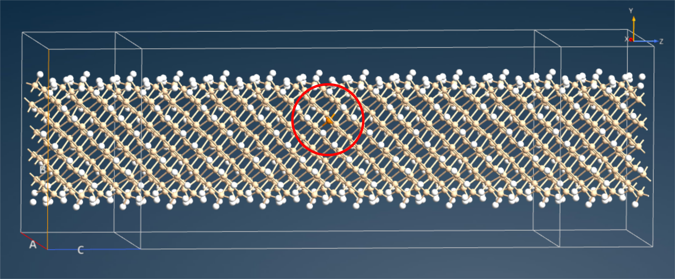
You can create an InAs nanowire by going back to the Builder window and follow these steps:
Repeat the InAs slab 6 times along the A-axis.
Change the lattice parameters so that the A-vector is 40 Å in the x-direction.
Passivate the nanowire in the same way as the slab, using the Custom Passivator.
Center the coordinates.
Send the structure to Script Generator and use exactly the same procedure as for the slab calculations with pseudo-hydrogen atoms.
Additionally,
Set the k-point sampling to (1,9,1)
Add Bandstructure and change the Brillouin zone route to “G, Y”.
Add Analysis/EffectiveMass and set Direction to “Cartesian”, and set (x,y,z)=(0,1,0).
Set the output file name to “InAs_nanowire.nc”.
Send the script to Editor and set the TB09 meta-GGA c-parameter to 0.936.
Finally send the script to Job Manager and run it.
Note that this calculation might take about an hour to finish.
When the calculation is finished you can run the Python script analyze_nanowire.py shown below in order to analyze the quality of the non-parabolic model .
importpylabasplfromNL.CommonConcepts.Configurations.Utilitiesimportfractional2cartesian#-------------------------------------------------------------------------# Model data#-------------------------------------------------------------------------# alpha parameter fitted to bulk InAsalpha_bulk=2.869# InAs bulk conduction band effective massmeff_bulk=0.028*electron_mass# Effective widths of nanowireDx=30*AngstromDz=30*Angstrom#-------------------------------------------------------------------------# Load DFT calcularted bandstructure and effective mass#-------------------------------------------------------------------------filename='InAs_nanowire.nc'# Read bulk configurationconfiguration=nlread(filename,BulkConfiguration)[0]# Read bandstructurebandstructure=nlread(filename,Bandstructure)[-1]# Read Effective masseffective_mass=nlread(filename,EffectiveMass)[0]meff=effective_mass.evaluate(band=1)[0][0][0]# Get the fractional kpointskpoints=bandstructure.kpoints()# Get reciprocal lattice vectors (used to convert frational k to cartesian k)G=configuration.bravaisLattice().reciprocalVectors()# K-points in cartesian coordinates, Ang^-1k_cart=fractional2cartesian(kpoints,G)# Get |k| as 1D arrayk=numpy.zeros(len(kpoints))forii,kiinenumerate(k_cart.inUnitsOf(Angstrom**-1)):k[ii]=(ki[0]**2+ki[1]**2+ki[2]**2)**0.5# Add unitk=k*Angstrom**-1# Get all the bandsbands=bandstructure.evaluate().inUnitsOf(eV)# Energies at the Gamma-pointE0=bands[0,:]# Index of conduction bandconduction_band_index=numpy.where(E0>0.0)[0][0]# Get the energies of the conduction bandconduction_band=bands[:,conduction_band_index]# conduction band minimumcbm=min(conduction_band)# Evaluate non-parabolic model bandstructureE_non_parabolic=(-1+(1+2*alpha_bulk*(hbar**2/meff_bulk*(k**2+numpy.pi**2/(Dx)**2+numpy.pi**2/(Dz)**2)).inUnitsOf(eV))**0.5)/(2*alpha_bulk)# Align conduction band minimum to DFTE_non_parabolic=E_non_parabolic-min(E_non_parabolic)+cbm# Evaluate parabolic model bandstructure and align CBME_parabolic=(0.5*hbar**2*k**2/meff_bulk).inUnitsOf(eV)+cbm# Ananlytical effective mass of slabm_slab=meff_bulk*(1+2*alpha_bulk*(hbar**2*numpy.pi**2/(meff_bulk)*(1/Dx**2+1/Dz**2)).inUnitsOf(eV))**0.5print''print'Analytical nanowire mass = %.4f m_e'%m_slab.inUnitsOf(electron_mass)print'DFT nanowire mass = %.4f m_e\n'%meff# Analytical band gap increasedelta_gap=(-1+(1+2*alpha_bulk*(hbar**2*numpy.pi**2/(meff_bulk)*(1/Dx**2+1/Dz**2)).inUnitsOf(eV))**0.5)/(2*alpha_bulk)print'Analytical band gap increase = %.4f eV'%delta_gapprint'DFT gap change = %.4f eV'%(1.548-0.354)print''pl.figure()pl.plot(k,conduction_band,'k',label='DFT conduction bands')pl.plot(k,bands[:,conduction_band_index+1:conduction_band_index+5],'k')pl.plot(k,E_non_parabolic,'r',label='Non-parabolic fit ')pl.plot(k,E_parabolic,'b',label='Parabolic fit')pl.xlabel('k (Ang.$^{-1}$)')pl.ylabel('Energy (eV)')pl.ylim([0,1.5])pl.legend(loc=0)pl.show()
As for the InAs slab, the lowest conduction band in the nanowire is much better described by the the non-parabolic model
than by the parabolic/effective mass model. Although the agreement between the non-parabolic model and the DFT band structure
is not quite as good as for the slab, it still provides a very reasonable estimate.