Transport calculations with QuantumATK
Version: 2015
This tutorial introduces you to one of the most important functionalities in QuantumATK, namely electron transport calculations.
The system you will investigate is a Zn|ZnO|Zn junction, which is selected for demonstration purposes, in order to make calculations relatively fast. However, this system does encapsulate many of the relevant and interesting physical effects present in more realistic devices, and these will be discussed in the tutorial.
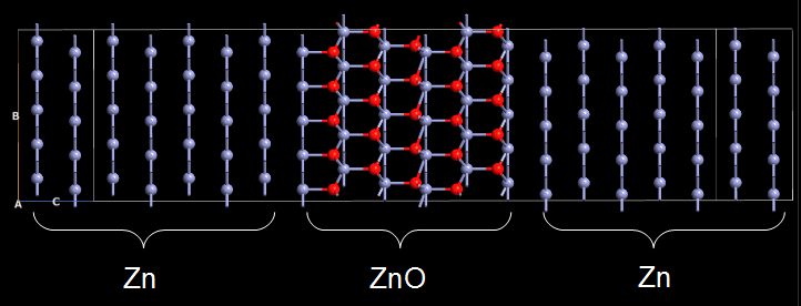
Fig. 131 The Zn-ZnO-Zn system to be studied in this tutorial. Note that the configuration is repeated 5 times along the B axis to improve the visual clarity.
Note
In order to run the calculations in this tutorial, you must have a license for the ATK-SE tight-binding engine. If you do not have one, you may obtain a time-limited demo license by contacting us via our website: Contact QuantumATK.
Attention
This tutorial was prepared using QuantumATK version 2016.3. Downloadable scripts and output files may therefore not work with QuantumATK 2015 and earlier.

Introduction
In this tutorial, the electronic structure of the Zn-ZnO-Zn junction will be calculated using a tight-binding (TB) model in combination with the non-equilibrium Green’s function (NEGF) technique for the actual calculation of the electron transport through this junction. A detailed description of technical aspects of the computational parameters and models can be found in the ATK Reference Manual.
To set up the calculations, you will use the graphical interface QuantumATK (QuantumATK). If you have never worked with QuantumATK before, it is highly recommended to first go through the Basic QuantumATK Tutorial to become familiar with the basics of how to operate the software.
You will here use a predefined device configuration, but we have many other tutorials that show you how to set up other device geometries.
Tutorial objectives
We will first introduce the central concepts involved in a device calculation, and then present a range of tools that can be used to analyze the electronic transport properties of the device.
After reading this tutorial and performing the calculations, you will be able to:
Understand the general concept of a device configuration.
Test convergence of physical quantities with respect to computational parameters.
Check if a given bulk configuration is suitable as an electrode.
Calculate the transmission spectrum at zero and finite bias voltage.
Analyze the transmission spectrum using the Transmission Analyzer.
Calculate and plot transmission eigenstates.
Calculate and plot the projected device density of states.
Calculate the potential profile (voltage drop) across the device.
Calculate the I–V curve and analyze it.
Geometry for transport calculations
The type of atomic configuration needed for an electron transport calculation is fundamentally different from the configurations used in atomic-scale simulations of periodic and finite structures. This is because an electron transport calculation requires open boundary conditions in the transport direction. Open boundary conditions make it possible for incident electrons coming from the source electrode to be partially transmitted through the central part of the device and end up in the drain electrode, and partially reflected back to the source.
One may see the device configuration as a combination of periodic and finite configurations, as shown in the figure below. The left and right bulk (periodic) electrodes (source and drain, in a transistor perspective) are attached to the central region of the device, which is finite (non-periodic) along the transport direction. The central region is often called the scattering region, because the charge carriers traveling between the two electrodes are scattered by changes to the physical and chemical environment in the central region, for example by interfaces and defects. The central region therefore determines the functionality of the device, while the left and right electrodes are modeled as perfect leads that connect the device to the external source and drain.
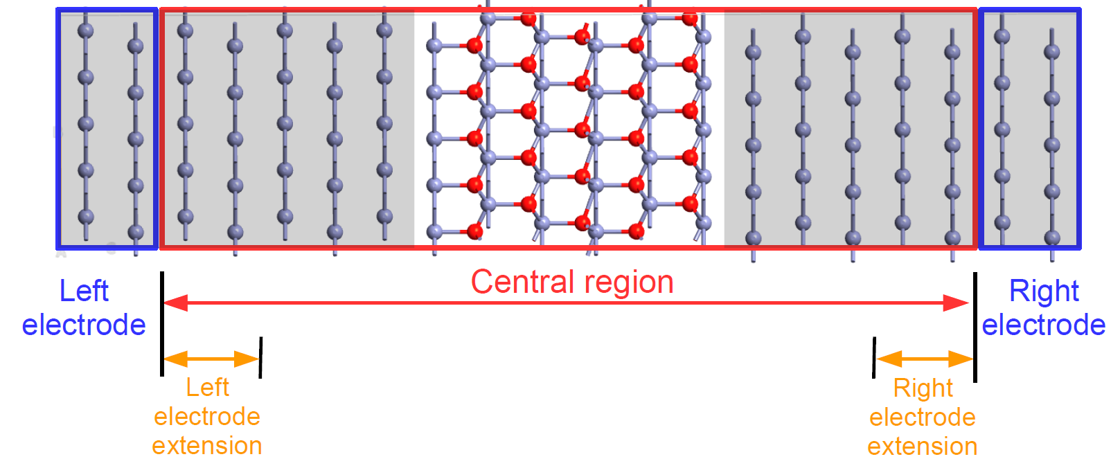
Fig. 132 A two-probe device configuration consists of two electrodes and a central region. Both ends of the central region, called the electrode extensions, must be exact replicas of the corresponding electrode structures.
For reasons of numerical stability during QuantumATK device calculations, there is a region in both ends of the central region where the element types and ionic positions are fixed to match the electrodes – these are the electrode extensions. Both must always be an exact replica of the corresponding electrode, and are therefore not allowed to change during geometry optimization of the device.
Hint
In both figures above, the device configuration is periodically repeated 5 times along the B axis (which points “up” in both figures) to improve visual clarity. However, just like in standard atomistic simulations one should always use device configuration with the smallest lateral unit cell area, taking advantage of any structural periodicity of the device in the A and B directions (orthogonal to the transport direction, C).
Important notes
The C-direction in the device configuration is the transport direction, meaning that the electrodes are always connected to the central region in this direction.
The electrodes are by default assumed to be periodic in the A and B directions, i.e., perpendicular to the transport direction. When simulating transport through 1D or 2D confined systems, such as wires, tubes, ribbons, and sheets, a sufficiently large vacuum padding should be added along the confined direction(s). This allows the electron density and electrostatic potential to decay correctly in the vacuum region, and this also avoids spurious interactions with repeated images of the system.
The central region can take many different forms. For example, it can be a metal–semiconductor–metal “sandwich”, as in this tutorial, a molecule between the two electrodes, or a piece of a nanotube or a graphene flake with a defect.
In the Zn|ZnO|Zn device treated here, the two electrodes are identical, but this is not a general requirement. For example, QuantumATK can easily simulate the electron transport through an interface between two different materials.
In addition to source and drain electrodes, QuantumATK supports inclusion of electrostatic gates for transistor simulations. This will not be covered here, but is addressed in several other tutorials.
The screening region
The central region should normally involve some structural inhomogeneity (interfaces, surfaces, molecules, defects, etc.) that leads to rearrangements in the electron density and hence in the self-consistent potential felt by the electrons. This electronic rearrangement may be further enhanced by structural relaxation effects inside the central region (excluding the electrode extensions, which are not allowed to relax). This deviation of the central region potential from the bulk electrode potential causes the electrons to be scattered, which will cause a voltage drop across the central region at finite bias.
Note
Simulating the transport properties of a perfectly periodic structure is only possible at zero bias (since there is no place for the voltage to naturally drop in a perfectly periodic structure, as there is no scattering), and can moreover be done in a simpler way, using just a periodic bulk configuration
The NEGF formalism assumes that the potential in the central region converges smoothly towards the electrode potentials, such that there is no scattering at the two electrode–central region interfaces. In the sketch of the Zn|ZnO|Zn device shown below, the Zn metal regions in both ends of the central region are on a gray background, just like in the electrodes, in order to indicate the so-called screening regions, in which the potential and charge rearrangements at the Zn–ZnO interfaces are screened and smoothly approach the electrode potentials. If the screening regions are shorter than the actual (physical) screening length of the system, spurious scattering may take place at the electrode–central region interfaces. This may give rise to poor convergence of the self-consistent calculation and inaccurate results in finite-bias calculations.
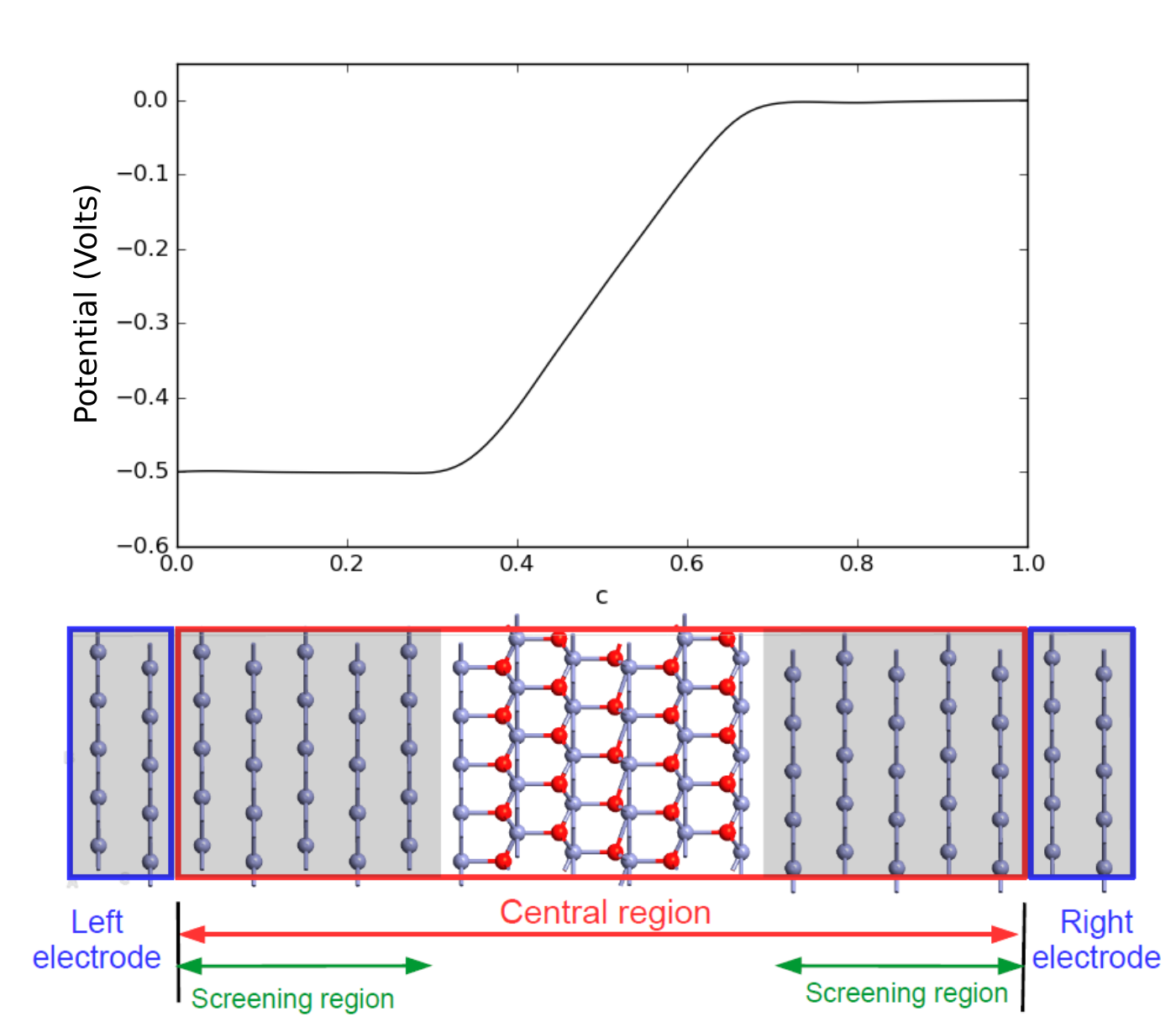
Fig. 133 Top: Electrostatic potential along the transport direction. Bottom: Device geometry. The screening regions in the left and right parts of the central region, indicated by gray background, must be longer than the screening length of the system to ensure a smooth transition between the potential of the central region and electrodes.
The figure above shows the potential profile due to an applied bias voltage of U = -0.5 Volt in the Zn|ZnO|Zn device considered here, meaning that the voltage on the left electrode is 0.5 V lower than that on the right electrode. Most of the “voltage drop” occurs in the ZnO region while the potential in the metallic screening regions is virtually flat, so no scattering takes place in these screening regions. In the section Finite-bias calculations you will reproduce this potential profile.
Attention
In systems with semiconductor electrodes, the screening length can be quite long, and a very long central region may be required before the potential approaches the bulk value. However, in most real situations, the semiconductor electrodes are doped, which brings the screening length down to manageable simulation sizes, provided the doping level is high enough.
Note
The entire treatment of electron transport is in this context coherent and elastic, i.e. there is no scattering by phonons.
The NEGF formalism assumes that the electrodes are in thermal equilibrium, which formally requires that the electrical current through the device is low. This always holds true at low voltage, and may also be a valid assumption at higher voltage, provided that the transmission probability through the central region is sufficiently low.
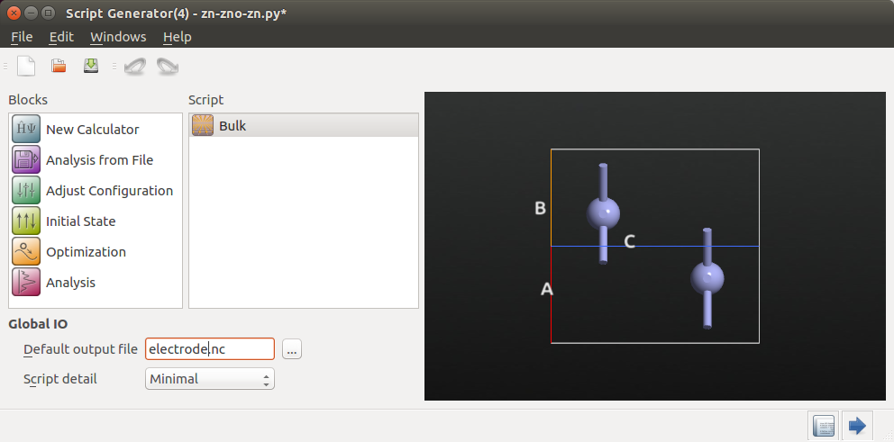
Getting started
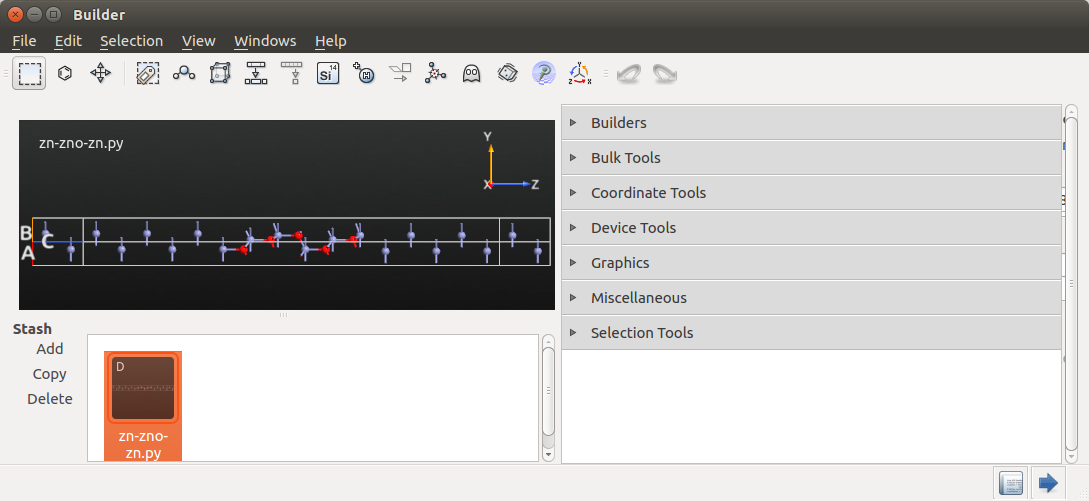
Start up QuantumATK and create a new project. You would normally use the
 Builder to create the device configuration, but here we
will use the Zn|ZnO|Zn device already defined in the QuantumATK Python script
Builder to create the device configuration, but here we
will use the Zn|ZnO|Zn device already defined in the QuantumATK Python script zn-zno-zn.py.
Download the script and save it in the project folder. It will then show up on in the Project Files list.
Drag the script onto the Builder to access a large palette
of tools for creating new configurations and modifying existing ones.
Convergence of electrode parameters
An QuantumATK device calculation is performed in multiple steps. First, the electrode(s) and the central region are treated as (periodic) bulk systems, and the self-consistent electron density is calculated for each of them. The device calculation is then started, using the central region bulk electron density as an initial guess, and matching the electronic structure at the two electrode/central region boundaries to that of the electrodes. Finally, the self-consistent electronic structure of the central region is determined, and thereby of the full device.
It is important to the procedure outlined above that the electrode bulk calculations are well converged, both in electrode lengths and numerical accuracy. The purpose of this section is to demonstrate the convergence of two very important numerical accuracy parameters; the mesh cut-off and the number of k-points in the transverse directions (A and B).
The convergence test will here be performed only on the left electrode, since the two electrodes are (physically) identical. In case the electrodes are not identical, the required mesh cut-off and k-point sampling should be determined separately for both of them. However, since these numerical parameters must be the same in the two electrodes in the device calculation, in the end they need to be chosen large enough that both electrodes are accurately described.
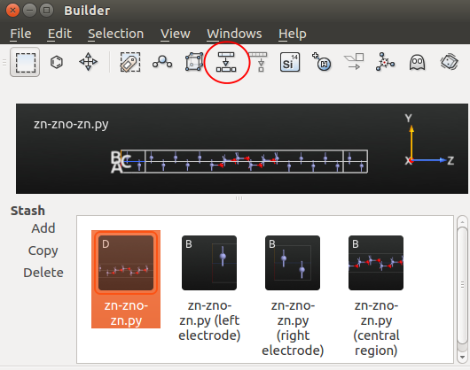
Split the device configuration
Use the Splitter tool  in the top toolbar to split the
device into electrodes and central region. This will add 3 new configurations
to the Stash, corresponding to the left and right electrodes and
the central region.
in the top toolbar to split the
device into electrodes and central region. This will add 3 new configurations
to the Stash, corresponding to the left and right electrodes and
the central region.
You can now highlight the left electrode configuration and use the  botton to send it to the
  Script Generator
and set up a range of bulk calculations for the electrode using different
density mesh cut-offs and k-point samplings to study the numerical convergence.
Script Generator
and set up a range of bulk calculations for the electrode using different
density mesh cut-offs and k-point samplings to study the numerical convergence.
For convenience, scripts have already been prepared for the calculations needed in the two convergence studies. In the following, you should simply download and run them.
Mesh cut-off
The first numerical parameter to converge is the density grid cut-off. This controls the density of the real-space grids in QuantumATK, which represent e.g. the electrostatic potential and real-space electron density. The density cut-off is specified as an energy \(E\); the corresponding distance between the grid points is given by
where \(m\) is the electron mass.
The script mesh_loop.py performs calculations of the ground state of the
electrode for different mesh cut-offs ranging from 2.5 Ha to 80 Ha. All
other numerical accuracy parameters are kept constant. The convergence
observable is the Fermi level (chemical potential) of the electrode.
The script simply loops over the mesh cut-offs, performs the calculation
for each value, and finally plots the results. Download the script, and
then run it using the  Job Manager. If you are not
familiar with the QuantumATK Job Manager, please refer to the tutorial
Job Manager for local execution of QuantumATK scripts. You can of course also run the script from
command line:
Job Manager. If you are not
familiar with the QuantumATK Job Manager, please refer to the tutorial
Job Manager for local execution of QuantumATK scripts. You can of course also run the script from
command line:
$ atkpython mesh_loop.py > mesh_loop.log
The plot will automatically appear once the calculations are done (in less than a minute). The plot is shown below. It is clear that the default 10 Ha mesh-cut-off for tight-binding calculations is a perfectly sufficient default, since the Fermi level changes by less than 10 meV when using larger values (which are computationally more expensive), and we will keep it for further calculations.
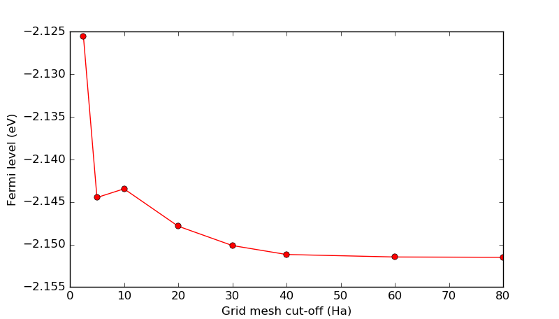
Attention
This weak dependence of computed quantities on the mesh cut-off is typical of tight-binding models. The same would generally not be true for DFT calculations, where the default mesh cut-off with the cheapest pseudopotentials is 75 Ha.
Transverse k-points
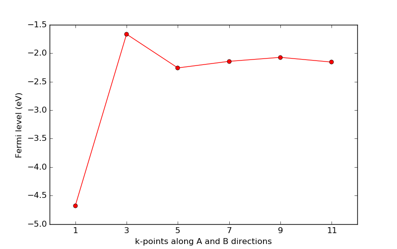
In the same fashion as above, you will now study the electrode Fermi level as a function of the number of k-points in the transverse directions (A and B), which are orthogonal to the transport direction (C).
The number of k-points in the transport direction should be quite large in a device calculation, so keep it at \(n_C\) = 51. All other numerical accuracy parameters should be kept at their default values, including the grid mesh cut-off (10 Ha).
Use the script kpts_loop.py for this convergence study. It is identical to the
one used above for the mesh cut-off, but loops over odd transverse k-points
in the range 1 to 11.
Download and run the script, which will produce the plot shown below. It is quite clear that the calculation with only 1 k-point along the A and B directions fails completely in describing the periodic Zn electrode bulk, while the calculations with 5 or more transverse k-points are much better.
Check the electrode geometry and size
After having performed the electrode calculator convergence tests, the final preparatory step consists of checking the electrode geometry, using the Electrode Validator plugin. This tool checks if the electrode configuration has the appropriate geometry (viz. if the C axis is parallel to the Z coordinate axis, and if the AB plane is perpendicular to C) and if the electrode is long enough along C.
You first need to do a ground state calculation for the electrode. Follow these steps to set up the calculation:
Open the
Builder and select the left electrode.
Then use the botton to send the electrode to
the Script Generator.
Change the default output file name to electrode.hdf5.
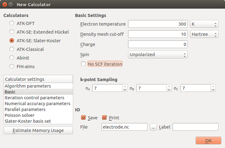
Add a
 New Calculator block and double-click it
to open it.
Select the Slater-Koster tight-binding calculator engine, make sure “No
SCF iteration” is not checked, and set up a 7x7x7 k-point grid.
New Calculator block and double-click it
to open it.
Select the Slater-Koster tight-binding calculator engine, make sure “No
SCF iteration” is not checked, and set up a 7x7x7 k-point grid.
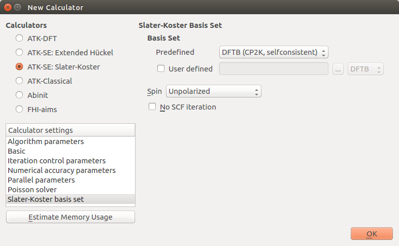
Finally, in the Slater-Koster basis set calculator settings, choose the self-consistent DFTB CP2K basis set.
Save the script as electrode.py and run the calculation. The script
can also be obtained here: electrode.py. The results should soon appear on the
LabFloor. Select the bulk configuration saved in the output file
(electrode.hdf5), open the Electrode Validator plugin in the right-hand
plugins toolbar, and click Check.
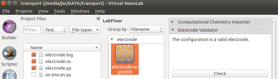
You should see a message saying The configuration is a valid electrode, indicating that the electrode geometry and length are fine. In case the electrode for some reason fails the check, a warning and an explanation will be presented.
Note
Whether an electrode is long enough in the C direction depends to some extend on the basis set used. The Electrode Validator uses the criterion that any discarded matrix elements of the Hamiltonian should not exceed 10-10 eV.
The reason for this is that only the nearest-neighbor interactions of the electrode along C are kept in the device calculation. Specifically, this is the interaction between the electrode and the electrode extension. This is necessary in order to describe the electrodes as semi-infinite rather than fully periodic along C).
If the electrode is deemed too short, you can still proceed with the device calculation, but, depending on how large the discarded matrix elements are, you risk that the calculation will not converge or that the results are inaccurate.
Tip
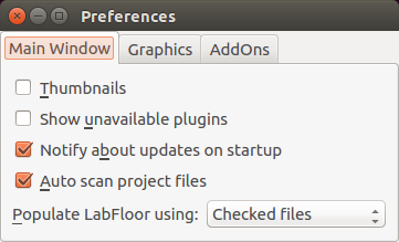
The screenshots for this tutorial have been made after unticking the option Show unavailable plugins in the menu in the QuantumATK main window. This causes QuantumATK to dynamically change the list of available plugins in the right-hand plugins bar, such that plugins that are not compatible with the selected LabFloor item are not shown.
Zero-bias analysis
Having confirmed that the geometry of the electrodes is indeed suitable
for QuantumATK device calculations, you are now ready to continue with the actual
transport calculations. In the Builder, Select the
Zn|ZnO|Zn device configuration, named zn-zno-zn.py, and send it
to the Script Generator.
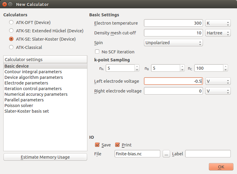
Transmission spectrum analysis
In the Script Generator, follow these steps to set up a script that calculates the electronic transmission spectrum of the Zn|ZnO|Zn device:
Change the default output file name to
zero-bias.hdf5.Add a
New Calculator block to the script.Add also the
 block.
Then edit the calculator settings by double-clicking
in the script:
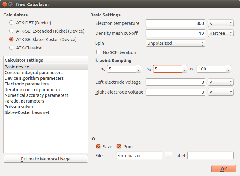
Choose the ATK-SE: Slater-Koster (Device) tight-binding calculator engine.
Set the transverse k-point samplings (along A and B) to 5.
Uncheck the box No SCF iteration to run a self-consistent calculation.
Verify that the Slater-Koster basis set is set to DFTB CP2K.
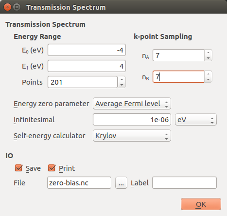
Next, edit the settings in the TransmissionSpectrum block:
Increase the energy window such that it ranges from -4 eV to +4 eV.
Increase the number of sampled energy points to 201.
Set the transverse k-point sampling to 7x7.
Change the self-energy calculator to Krylov.
Note
The density of energy points will determine the accuracy of the computed current at finite bias.
For the energy window, it is recommended to choose a wide interval at zero bias to get a picture of where the transmission peaks are located, but for finite bias, a proper convergence study should be performed, since a too wide energy spacing (too low density of energy points) may mean that narrow peaks in the transmission spectrum are not captured.
The k-point sampling used in the transmission analysis (and in most post-SCF analysis calculations) does not need to be the same as used in the calculator. Typically, you need more k-points in the transmission analysis than in the SCF calculation.
The Krylov self-energy calculator is chosen here because it is the fastest method available, but in some cases it can give negative transmission values due to some approximations made.
The script is now ready, so save it as zero-bias.py. If needed,
you can also download the final script here: zero-bias.py.
Running the calculation
Execute the script using either the Job Manager
or from command line. The calculation should finish in a few minutes.
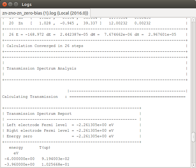
You should have a look through the job log file to follow the progress of the device calculation. You will see that the following sequence of calculations are carried out:
Left electrode SCF (bulk).
Right electrode SCF (bulk).
Device SCF (NEGF).
Transmission spectrum analysis.
Congratulations! You have now performed a complete transport calculation with QuantumATK. The basic work flow is similar for all transport calculations. Please proceed to the next section to visualize and analyze the results.
Transmission Analyzer
The calculation output should now have appeared on the LabFloor.
Locate and select the file zero-bias.hdf5. It contains two objects:
 DeviceConfiguration contains the two-probe device
configuration and the self-consistent state of the attached calculator.
DeviceConfiguration contains the two-probe device
configuration and the self-consistent state of the attached calculator.
 TransmissionSpectrum contains all information
about the computed transmission spectrum, including settings and results.
TransmissionSpectrum contains all information
about the computed transmission spectrum, including settings and results.
Select the TransmissionSpectrum object, and click the Transmission Analyzer in the right-hand panel bar.
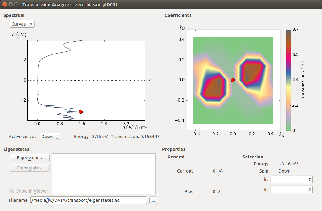
The Transmission Analyzer plugin opens. On the left, named Spectrum, is shown the k-point averaged transmission spectrum as function of energy. The average Fermi energy of the two electrodes is set to zero and indicated with a dashed line. It is evident that there is a broad energy range from -2.5 eV to +2.5 eV with very low transmission values. This corresponds to the band gap in the semiconducting ZnO.
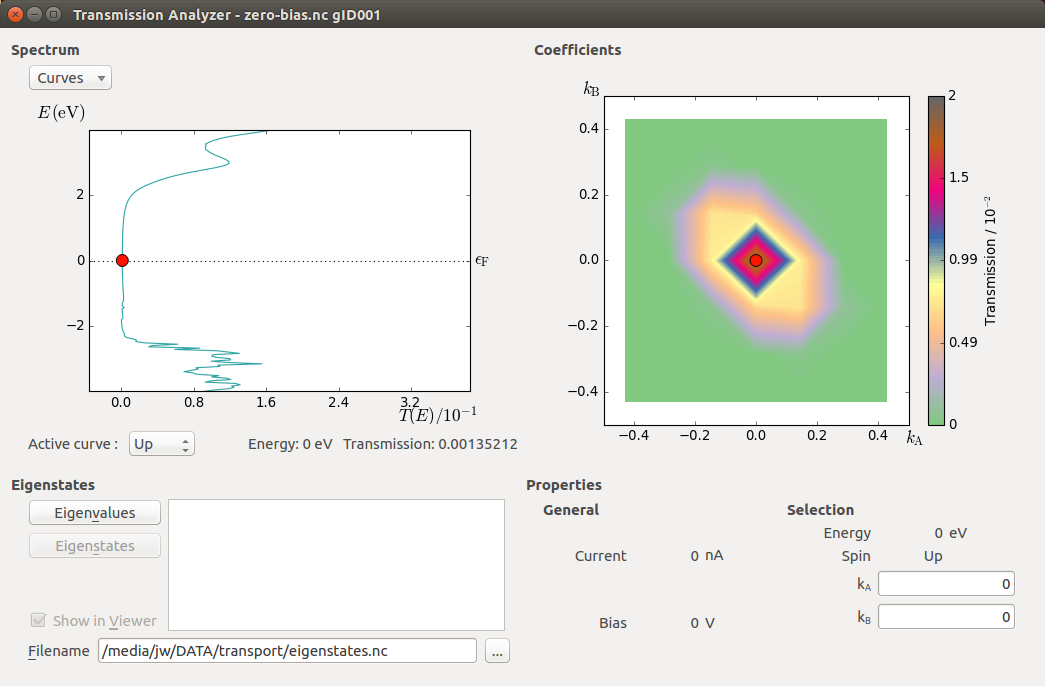
The transmission and energy values in the point marked by the red dot are shown below the plot. You can use the mouse to move the dot along the \(T(E)\) curve and read off the values. The Curves drop-down menu lets you select the spin components to be plotted. Note that the transmission for spin types X, Y, and Z are only non-zero for calculations with noncollinear spin.
At any particular energy (defined by the red dot), the total transmission is computed as an average over the transmission coefficients in the sampled k-points. The right-hand plot, named Coefficients, shows an interpolated contour plot of the transmission coefficients vs. reciprocal vectors \(k_A\) and \(k_B\).
In the figure above, it is clear that the main contributions to electronic transmission through the Zn|ZnO|Zn device at the average Fermi level come from k-points around the \(\Gamma\)-point, where \(k_A=k_B=0\). The situation is very different at other energies, such as e.g. \(E\) = -3.16 eV, as shown in the figure below.
Tip
By increasing the number of k-points sampled in the transmission spectrum calculation, the resolution of the contour plot can be improved – and thereby also the accuracy of the total transmission spectrum. In many devices, a large number of k-points may be required to obtain a converged spectrum.
Transmission eigenstates
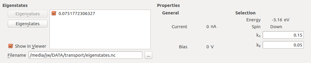
By clicking on the contour plot you can also move the red dot to a desired k-point. The chosen k-point is shown in the Selection box. At a particular energy and spin (chosen in the Spectrum plot) and a particular k-point (chosen on the Coefficients contour plot) you can obtain the transmission eigenvalues and eigenstates:
Select a k-point with high transmission value; (\(k_A\), \(k_B\)) = (0.15, 0.05) at energy -3.16 eV.
Click Eigenvalues in the lower left part of the window.
The transmission eigenvalues for the selected energy, k-point and spin are calculated, and after a couple of seconds the eigenvalues are listed.
Hint
If several transmission channels contribute to the transmission, more than one eigenvalue will be shown. Each eigenvalue is restricted to the range [0, 1], but the sum of the eigenvalues, which equals the k-point resolved transmission \(T(E,\mathbf{k})\), may be larger than 1, just like the total transmission \(T(E)\) can be.
You can now calculate and visualize the transmission eigenstate for each eigenvalue:
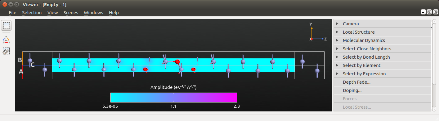
Select an eigenvalue and click Eigenstates. The 3D viewer opens after a few seconds.
Select the Cut plane plotting type and click OK.
The  Viewer now displays the Zn|ZnO|Zn device configuration
and a cut-plane representation of the transmission eigenstate throughout
the device central region.
Viewer now displays the Zn|ZnO|Zn device configuration
and a cut-plane representation of the transmission eigenstate throughout
the device central region.
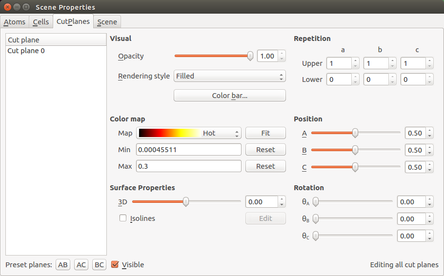
Next, edit the visual properties of the cut-plane to focus the color palette on the finer features of the eigenstate:
Open the Properties editor in the right side of the Viewer.
In the CutPlanes tab, change the colormap to “Hot”, then click Fit, and enter 0.3 for the maximum eigenstate value to be visualized.
The cut-plane visualization should now look as illustrated below. The eigenstate corresponds to a scattering state coming from the left electrode and traveling towards the right. The eigenstates will therefore always have a large amplitude in the left-hand part of the central region. Eigenstates with a relatively high transmission eigenvalue will also have a relatively large amplitude in the right-hand part of the scattering region. This simply reflects the relatively high transmission probability of an incoming state (at a specific energy, spin, and k-point) that attempts to travel through the central region and into the right electrode.
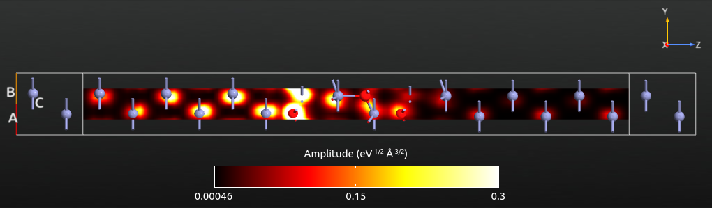
The transmission eigenstates in the left part of the scattering region are composed of an incoming (right-moving) and a reflected (left-moving) state. This leads to interference effects, which can be observed in the figure above: The eigenstate amplitude around the first Zn atom is relatively small due to destructive interference between the incoming and reflected states. To the right of the ZnO, the eigenstate consists only of the transmitted (right-moving) states, and no such interference effects are observed.
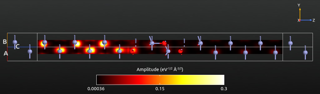
Try yourself to plot the transmission eigenstate at the Fermi level (energy E = 0 eV) and \(k_A=k_B=0\). By adjusting the plot properties you can get a plot similar to the one shown below. Now the eigenstate has a vanishing amplitude in the middle and right parts of the scattering region, due to the low transmission eigenvalue, i.e. only a tiny part of the scattering eigenstate is transmitted, and most of it is reflected at the Zn–ZnO interface.
Tip
If you instead plot the transmission eigenstate as an isosurface, the isovalue corresponds to the magnitude of the wave function, and the phase is used to color the isosurface.
Convergence of k-points for transmission spectrum
As already mentioned, more k-points are typically needed to obtain a
well-converged transmission spectrum than for the SCF calculation. As an
example, consider the figure below, which shows the total transmission
(averaged over all k-points) evaluated at three different energies and
plotted as function of the number of k-points in the transverse A and B
directions. The figure was generated using the script transmission_kpts.py.
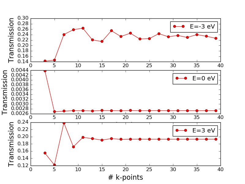
Fig. 134 Total electronic transmission vs. the number of k-points in the transverse directions for the Zn|ZnO|Zn device evaluated at three different energies: -3 eV (top), 0 eV (middle), and 3 eV (bottom).
The transmission converges very differently at different energies. While the transmission at the Fermi energy is converged with just 5 or 7 k-points in the A and B directions, at -3 eV and +3 eV it looks like at least 13 k-points are needed.
You may recall from above that the transmission spectrum has many sharp peaks in the region around -3 eV. It is typically such, that many k-points are needed when sharp features are present. However, there may also be isolated peaks that are “hidden” by too low k-point density, so one really needs to study the k-resolved transmission plot to get an idea of the needed k-point sampling.
Additionally, in a region with many (sharp) transmission peaks as function of energy, a large number of energy points are required to converge the integral over energy needed to compute the current.
Further analysis
This section will introduce some further ways to analyze the zero-bias calculation. An important feature in QuantumATK is that you do not have to define all analysis quantities from the outset; you can always calculate additional quantities without having to redo the self-consistent calculation from scratch.
You will now compute the device density of states (DDOS) of the Zn|ZnO|Zn configuration, and the electrostatic difference potential:
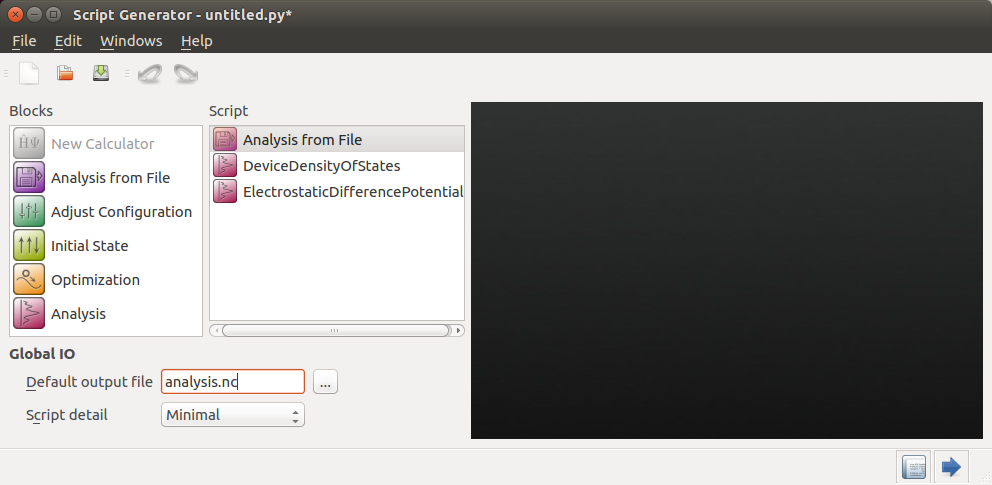
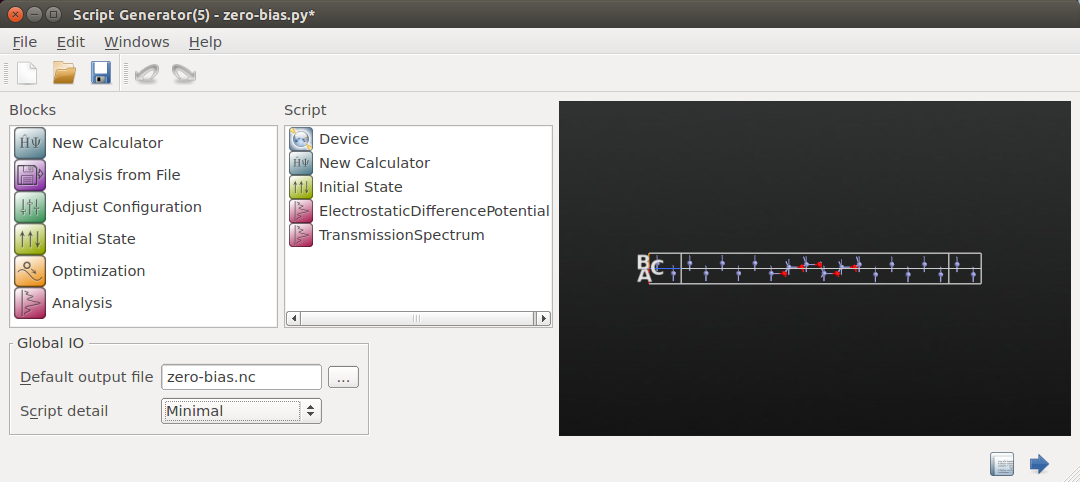
Open a new
Script Generator window.Change the output file name to
analysis.hdf5, and add three blocks to the script: Analysis from File
- DeviceDensityOfStates
- ElectrostaticDifferencePotential
Open the
Analysis from File block. This is the part
of the QuantumATK script that is responsible for reading the converged state of the
zero-bias calculation. You need to specify which file and which
saved configuration you want to base the following analysis on
(there may be several configurations in a single file).Select the saved file
zero-bias.hdf5– the configurations stored in that data file are then automatically detected and listed. Only one configuration is in this case available; it has object ID “gID000”. Make sure that configuration is ticked, and click OK.
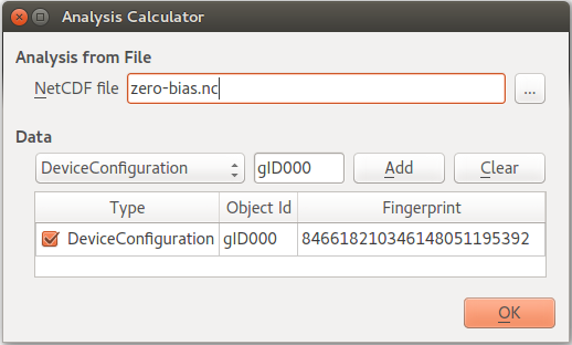
Tip
The ID number of each object is indicated below its icon on the LabFloor. To distinguish different configurations in the same file, you can use the General information plugin to inspect the most important parameters of the calculation.
Next, edit the
DeviceDensityOfStates settings, which should
be similar to the settings used for computing the transmission spectrum:energy range from -4 eV to +4 eV with 201 points.
7x7 k-point sampling.
Krylov self-energy calculator.
No changes need be made to the
ElectrostaticDifferencePotential analysis.
The analysis script is now ready. Save it as analysis.py and execute it
using the Job Manager or from command line – it takes only a
few minutes to run. You can also download the script here: analysis.py.
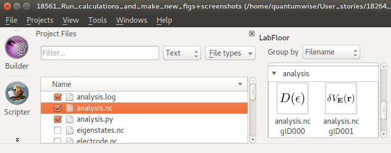
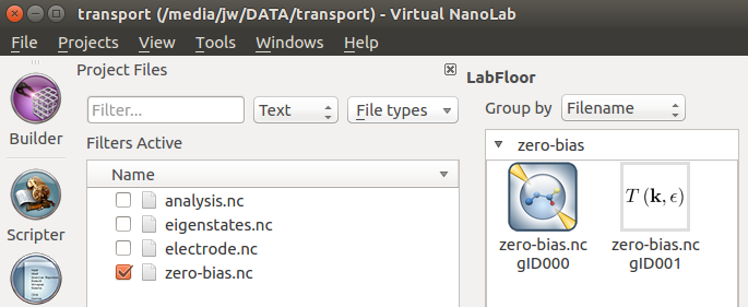
When the job is done, observe that the analysis results have appeared on the LabFloor:
 DeviceDensityOfStates
 ElectrostaticDifferencePotential
Device density of states
Select the DeviceDensityOfStates object and click 2D plot in the right-hand plugins bar to visualize it.
The 2D Plot window opens with the DDOS plottet on the left. The right-hand panel allows you to also visualize the configuration and select atoms and orbitals to project the DOS onto:
Under Configuration HDF5 File, select the output file
zero-bias.hdf5for visualizing the device configuration (which is not saved inanalysis.hdf5).Under Projection selector, select atom indices 8,9,10,11 in order to preject the DOS onto the middle part of the ZnO layer.
Then zoom in on the projected DOS like shown in the figure below.
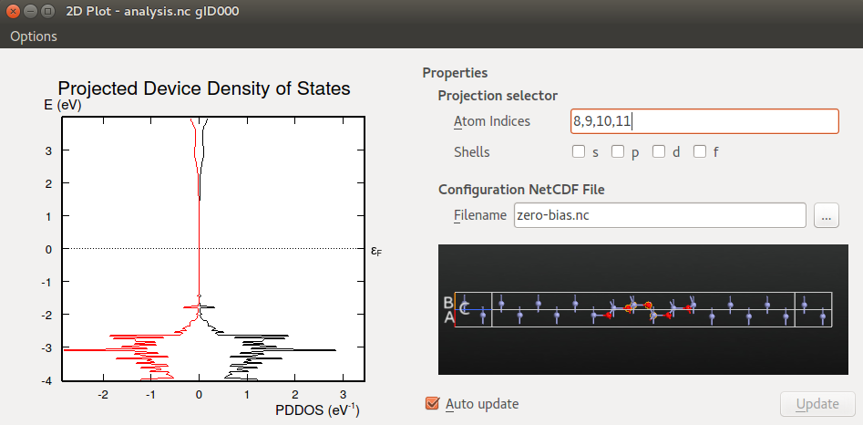
You should notice that the shape of the DDOS resembles the shape of the transmission spectrum analyzed above: Both plots show a broad energy region around the Fermi energy with low values, reflecting the semi-conducting nature of ZnO; for energies below -2 eV there are many sharp peaks; finally, both the transmission spectrum and the DDOS display a broad peak around +3 eV. The correspondence between the transmission spectrum and DDOS is a very general feature often observed in device calculations.
Electrostatic difference potential
The ElectrostaticDifferecePotential object contains a 3D grid that represents the difference between the electrostatic potential of the self-consistent valence charge density (the solution to the Poisson equation with this density) and the electrostatic potential from a superposition of atomic valence densities. You will use this object later when calculating the voltage drop.
You can of course use the Viewer to visualize such 3D grids,
just like you did for the transmission eigenstates a few sections up.
Another way
to visualize a quantity represented on a 3D grid is to use the 1D Projector.
With this tool you can project a potential or density along a certain direction,
integrated or averaged over the two directions perpendicular to it. For devices,
it is often most interesting to plot the potential along the transport direction
(C) and to average over the A and B directions.
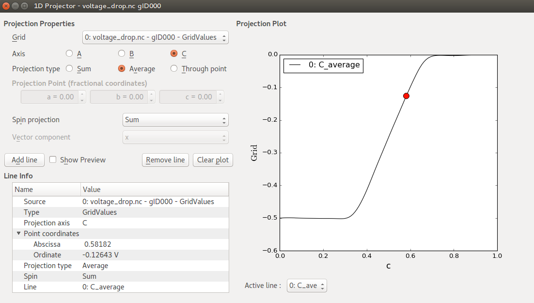
Select the ElectrostaticDifferencePotential object on the LabFloor, and open the 1D Projector from the right-hand plugins bar.
Change “Projection type” to Average and click Add line.
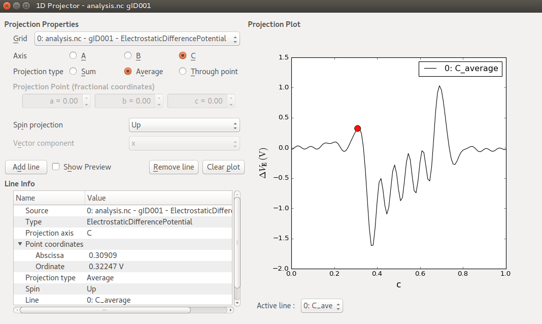
You should now see a plot like shown in the figure above, where the electrostatic difference potential, \(\Delta V_E\), is plotted against the fractional C-coordinate (ranging from 0 to 1).
A significant charge transfer seems to take place at both Zn–ZnO interfaces, causing the self-consistent electrostatic potential to differ significantly from that of the atomic valence densities. In the metallic Zn regions near the electrodes, oscillations are rather small, indicating that the self-consistent charge distribution is not much different from the atomic valence charges in those regions.
Finite-bias calculations
All calculations performed so far have been with zero voltage on the left and right electrodes, i.e. at zero bias. In this section you will use the zero-bias calculation as a starting point for finite-bias calculations, where the left and right electrode voltages are different. This shifts the left and right electrode Fermi levels relative to each other – a basic mode of operation for electronic devices.
The recommended method for obtaining fast and reliable SCF convergence for finite-bias QuantumATK transport calculations is to start out from a zero-bias calculation and change the bias in small steps. You will now perform a device calculation at -0.5 V bias.
Set up the calculation
In the QuantumATK Project Files list, tick the file zero-bias.hdf5 to see its
contents on the LabFloor, and drag the DeviceConfiguration (gID000) onto the
Script Generator. This will setup the Slater-Koster
calculator parameters identically to those used for the zero-bias calculation.
Add three blocks to the script:  Initial State,
,
and .
Initial State,
,
and .
Then change the default output file to finite-bias.hdf5, and open the
New Calculator to apply a bias:
Set the Left electrode voltage to -0.5 V.
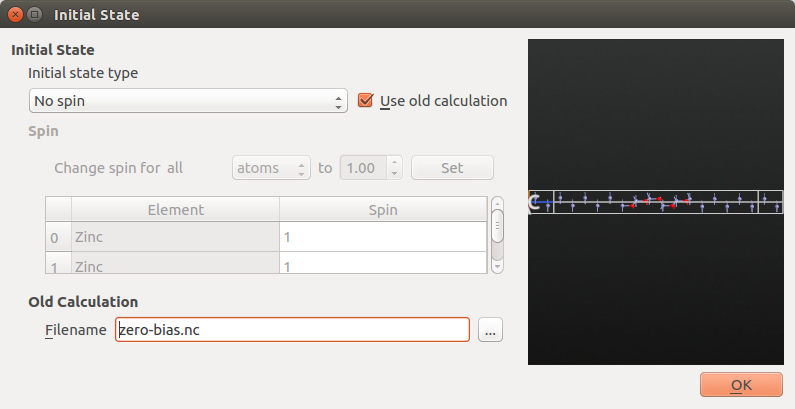
Next, open the Initial State block to instruct QuantumATK to
use the zero-bias state as an initial guess for the finite-bias calculation:
Tick Use old calculation, and choose
zero-bias.hdf5as the filename of the Old Calculation.
Lastly, set up the TransmissionSpectrum parameters identically
to those used for the zero-bias calculation:
Energy window of -4 eV to +4 eV with 201 energy points.
7x7 transverse k-points.
Krylov self-energy calculator.
Save the script as finite-bias.py and run it. The calculation will take
a little more time than the zero-bias calculation. If needed, you can download
the final script here: finite-bias.py.
Note
Electrode voltages and current In a zero-bias calculation, the local chemical potential is constant throughout the device, including the electrodes. Applying a potential difference \(U = V_\mathrm{L} - V_\mathrm{R}\) between the electrodes is identical to shifting the electrode Fermi levels with respect to each other,
where \(\mu_\mathrm{L}\) and \(\mu_\mathrm{R}\) are the left and right electrode Fermi levels, respectively, and \(e\) the (positive) elementary charge.
The bias voltage \(U\) is therefore positive when the applied potential on the left electrode is higher than on the right electrode. This situation is also called forward bias, and implies that the chemical potential in the left electrode is moved down such that \(\mu_\mathrm{L} < \mu_\mathrm{R}\). Conversely, under reverse bias, we have \(V_\mathrm{L} < V_\mathrm{R}\), and therefore a negative bias voltage and opposite ordering of the chemical potentials, \(\mu_\mathrm{L} > \mu_\mathrm{R}\).
A positive current corresponds to charges moving from left to right, meaning that electrons move from right to left (since electrons have a negative charge). The current is therefore positive under forward bias and negative under reverse bias, so you should expect to get a negative current with the bias setting specified above.
Type |
Bias voltage |
Electrode potentials |
Chemical potentials |
Current |
|---|---|---|---|---|
Forward |
\(U>0\) |
\(V_\mathrm{L} > V_\mathrm{R}\) |
\(\mu_\mathrm{L} < \mu_\mathrm{R}\) |
\(I > 0\) |
Reverse |
\(U<0\) |
\(V_\mathrm{L} < V_\mathrm{R}\) |
\(\mu_\mathrm{L} > \mu_\mathrm{R}\) |
\(I < 0\) |
Attention
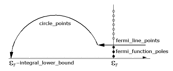
NEGF contour integral For finite-bias calculations, a potentially important convergence parameter is the Real axis point density, which is specified under Contour integral parameters. This parameter determines how many energy points are used when integrating the left and right spectral density matrices along the real energy axis between the chemical potentials of the left and right electrodes. For the present calculation you can proceed with the default value, but be aware that a convergence test of this parameter should in general be performed.
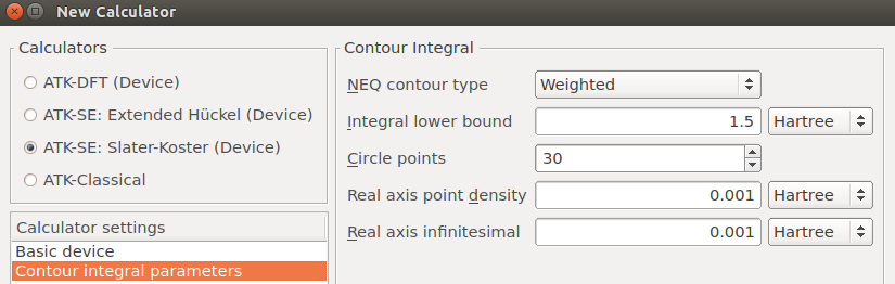
The settings Integral lower bound and Circle points are another important set of parameters. The NEGF contour integral needs to include all eigenvalues on the energy axis, but these are in general not known a priori. The default lower bound for the integral is 1.5 Ha below the Fermi level, but for DFT calculations with “hard” pseudopotentials (many valence electrons, possibly semi-core states), there may well be eigenvalues deeper than that. In that case, the Integral lower bound should be increased, and possibly also the number of circle points. Poor device SCF convergence is often due to such issues.
Analyzing the results
Go to the QuantumATK main window and open finite-bias.hdf5 on the LabFloor.
Use again the Transmission Analyzer to plot the transmission spectrum.
Notice that the chemical potential of the left and right electrodes are
separated by the bias of 0.5 V and distributed evenly around the average
electrode Fermi levels, which still is the energy zero reference. Also,
you can see that there is a (very small) negative current flowing in
this system, consistent with the direction in which the bias was applied.
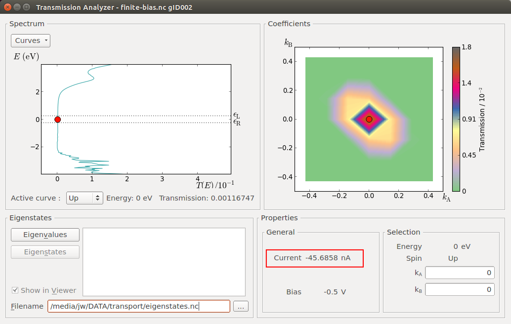
The finite-bias transmission looks essentially the same as found for zero bias. Recall from the analysis in section Device density of states that you found similar shapes of the ZnO DDOS and the transmission function. The shape of the transmission function is thus in this system largely determined by the density of states of the ZnO, and not so much by the electronic structure of the electrodes. Since the transmission values are very small in the bias window, the current is low and hence the change in DDOS in the ZnO is small. This is not necessarily the case in other systems, especially not if the bias is large enough to bridge the band gap of the scattering region.
Voltage drop
Your next task is to calculate the potential profile along the device transport direction at finite bias, also known as the voltage drop or the induced electrostatic potential. This can be computed as the difference between the electrostatic difference potentials at finite and zero bias,
Hint
Each electrostatic difference potential is the difference between the electrostatic potential of the self-consistent valence charge density and the electrostatic potential from a superposition of atomic valence densities. Since the atomic valence charge densities are the same for the zero and finite bias calculations, the calculated difference, \(\Delta V_E({\bf r})\), is the potential due to the differences between the two self-consistent charge densities, which is exactly the voltage drop.
The QuantumATK Grid Operations plugin is a very convenient tool. It allows you
to perform arithmetic operations on 3D grids, such as addition and subtractions
of one grid from another, and also multiplication and division. You will now
use the plugin to compute \(\Delta V_E({\bf r})\), save it in a file,
and then plot it in the Viewer:
By default, the Labfloor groups all items by filename. Change the option Group by to Item Type.
Then select the two ElectrostaticDifferencePotential items, and open the Grid Operations tool.
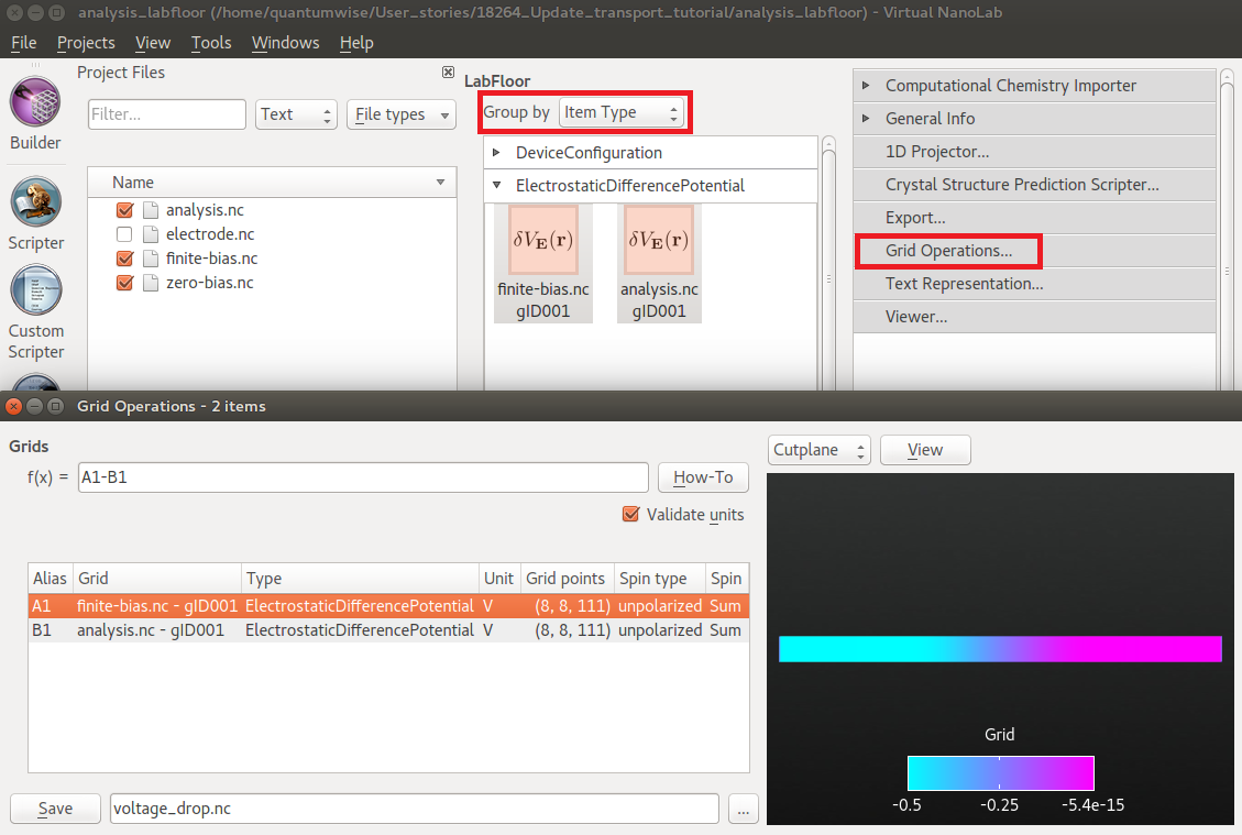
In the Grid Operations tool, the grids are assigned aliases. Depending on the order in which you selected the two items, the finite and zero bias potentials will be called A1 and B1, or opposite. To compute the voltage drop (the induced potential), subtract the zero-bias potential from the finite-bias potential by entering A1-B1 (or opposite) in the box next to f(x)= and press Enter on your keyboard.
You can then immediately plot the result as a cut-plane or an iso-value contour in the 3D window to the right, and/or save the difference grid in a new HDF5 file by clicking the Save button in the lower left corner.
Save the difference grid as voltage_drop.hdf5, and observe the GridValues
object appear on the LabFloor.
Note
 GridValues is a general container for quantities
represented on 3D grids.
GridValues is a general container for quantities
represented on 3D grids.
Select one of the DeviceConfigurations and open it with
the Viewer.
Then drag and drop the GridValues object onto the Viewer canvas in order
to visualize it on top of the device configuration. Choose the Cut-plane
visualization type, and set the color map to RGB.
The visualization should look like shown below. The potential drop occurs in the center of the device region, around the ZnO layers, showing that this is where scattering of the electrons takes place.
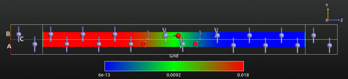
For a more quantitative analysis, open the saved difference grid with the 1D Projector, choose Average as projection type, and click Add line. You should now see a plot like the one shown below. The potential values are given in Volt. The right-to-left potential drop is -0.5 V, which is exactly the applied bias voltage.
Also note that the induced potential is flat towards the electrodes, indicating that the Zn layers in the left and right ends of the central region provide sufficient screening.
I–V curve
The last finite-bias device analysis in this tutorial is the I–V curve.
You will first compute it using the  IV Characteristics
analysis in the Study Objects, and then visualize it
using the IV-Characteristics Analyzer plugin.
IV Characteristics
analysis in the Study Objects, and then visualize it
using the IV-Characteristics Analyzer plugin.
Attention
The
analysis has been implemented since the O-2018.06 version. If you use an older version,
you can use the object instead.
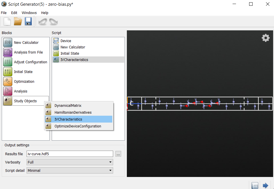
Calculations
Drag and drop the zero-bias.hdf5 or zero-bias.hdf5 file
onto the Scripter. It automatically keeps the settings of
the zero-bias calculation. Now do the following:
Add the
Initial State block.Add the
block.Change the default output filename to
iv-curve.hdf5.
Next, open the Initial State block to instruct QuantumATK to
use the zero-bias state as an initial guess for the finite-bias calculation:
Tick Use old calculation, and choose
zero-bias.hdf5orzero-bias.hdf5as the filename of the Old Calculation.
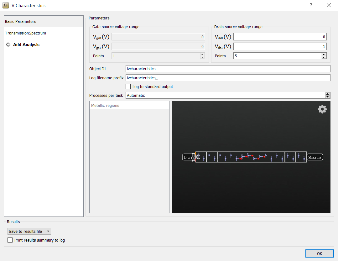
Edit the IVCharacteristics block:
Decrease the number of voltage points to 5 (for speed).
The QuantumATK Python script is now done. Save it as iv-curve.py and
execute it using the Job Manager or from the command line.
This calculation will take some time, because a self-consistent calculation
and a transmission spectrum analysis must be done at each bias point,
so probably around 10 minutes in 16 cpus.
If needed, you can download the script here: iv-curve.py. If you do not want
to perform the calculation yourself, you can also just download the results:
iv-curve.hdf5.
Visualization
The calculation should now be done, and the  IVCharacteristics
data item should now be included in the
IVCharacteristics
data item should now be included in the iv-curve.hdf5 output file.
Five new output files were also created, prefixed ivcharacteristics;
they contain the log file at each bias point.
Note
The IVCharacteristics item contains the calculated I–V curve,
including the transmission spectra computed at each bias voltage.
Select the IVCharacteristics item on the LabFloor and
click the IV-Characteristics Analyzer tool in the right-hand plugins bar.
The I–V curve is plotted in the window that pops up.
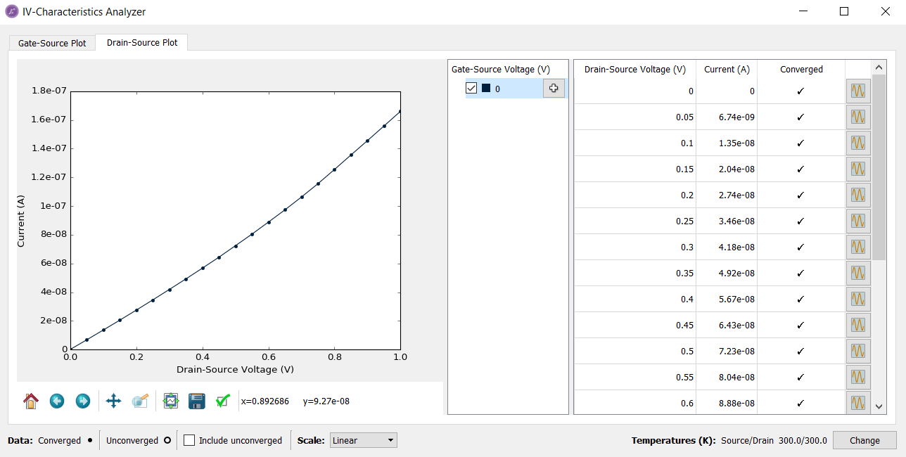
Select the Drain-Source Plot tab and choose the scale of current by right-clicking and choosing Customize. Change the maximum for the y-axis to 1.8e-07 to get the plot shown below.
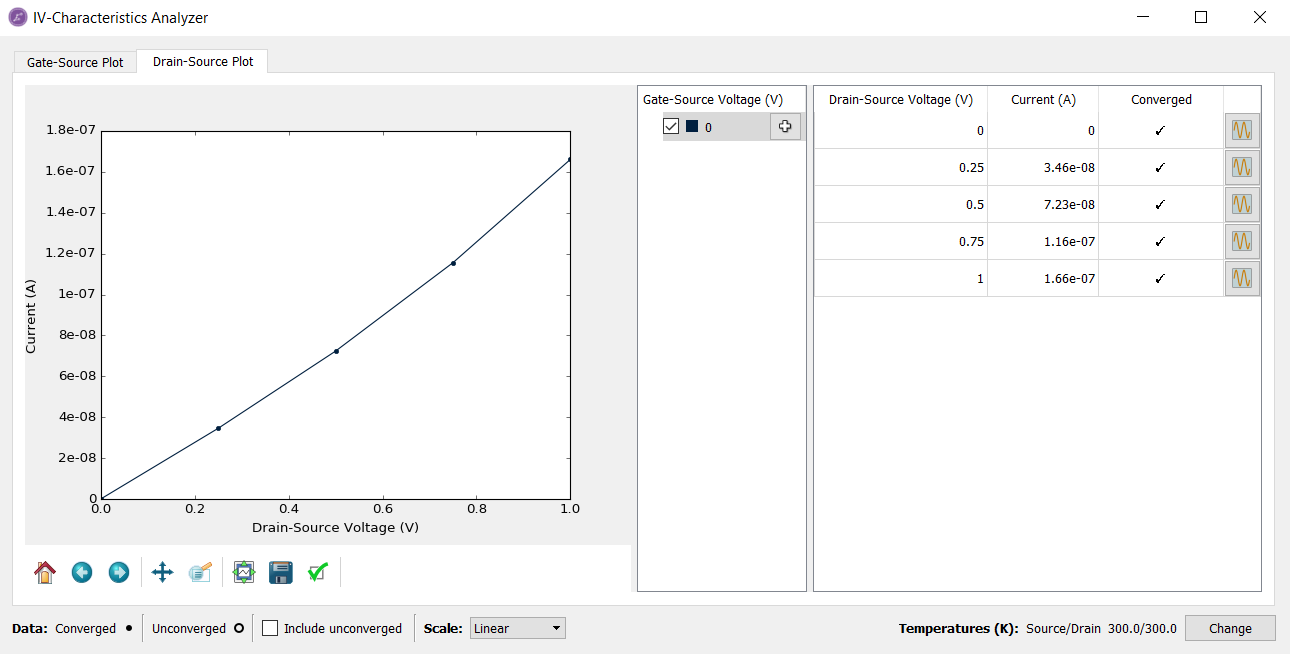
The table in the IV-Characteristics Analyzer shows the current and status
of convergence at each finite voltage.
Once you click the right-hand side plot icon ( ) in the table for the first time, the Analyzer will load in the Transmission spectra from the file. You can the visualize the transmission spectrum
corresponding to a specific bias voltage point by clicking the icon and choosing Transmission spectrum.
) in the table for the first time, the Analyzer will load in the Transmission spectra from the file. You can the visualize the transmission spectrum
corresponding to a specific bias voltage point by clicking the icon and choosing Transmission spectrum.
A somewhat finer bias-point sampling would yield a more accurate current.
To this end, you should increase the number of bias points
to 21, for example, and re-run the script with IVCharacteristics study object. It will automatically re-calculate the new points. You can also download the
result here: iv-curve_fine.hdf5.
Note
The IVCharacteristics study object enables
addition of more bias points. Simply add more voltage points in the
IVCharacteristics object with the same calculator settings,
then run it in the existing output file directory.
The IVCharacteristics recognizes the existing bias points smartly,
and just runs the additional voltage points. It will be faster and
not waste the computational cost. See also the dedicated tutorial: Electrical characteristics of devices using the IVCharacteristics study object for more information.
The finely sampled I–V curve is illustrated below. Compare it to the coarsely sampled one shown above even though the IV-curves look very similar.
Summary
You have now been introduced electronic transport calculations with QuantumATK.
You have gained an understanding of the general structure of a device geometry, and can continue with setting up other device geometries.
You have learned about important convergence parameters, such as transverse k-points, density mesh cut-off energy, and NEGF contour integral settings.
You are now able to calculate the transmission spectrum at zero and finite bias voltage, and analyze the results using the Transmission Analyzer.
You have also been introduced to other analysis tools like projected device density of states, electrostatic difference potential, transmission eigenvalues and eigenstates, and I–V curve using the IV characteristics study object.
You are also able to visualize 3-dimensional objects with the 3D Viewer or by using 1D projections.
Tip
What’s next? Now that you know the basics of electron transport calculations, it would be wise to continue to the tutorial Phonons, Bandstructure and Thermoelectrics to learn about simulating phonon transport with QuantumATK.