Building a Si-Si3N4 Interface
QuantumATK: Complex Interface
Platforms:
Links: American Mineralogist CSD, Crystallography Open Database
|
|

Note

The β-Si3N4(0001)/Si(111) interface was as studied in detail in Ref. [1], and we will use the geometry proposed in that work. An earlier model for the crystalline interface of β-Si3N4(0001)/Si(111) was proposed by Zhao and Bachlechner, but that model contained dangling bonds, which is not consistent with experimental findings. The interface you will build here has all bonds saturated.
To find an appropriate input structure for β-Si3N4, visit the American Mineralogist Crystal Structure Database and enter “si3n4” in the General Search box. This will return three matches - the one entitled “Si3N4”, by P. Yang et al., is the β-Si3N4 you are looking for (the other two are nierite, α-Si3N4). Click “Download CIF data” and save the CIF file in a convenient location.
Alternatively, you can use the Crystallography Open Database, and enter “si3n4” in the text search field.
In either case, be sure to download the structure with space group “P 63/m”.
Rename the downloaded file to Si3N4.cif, to make it easier to identify it.

Preparations: Two crystals
Step 1: In QuantumATK, open the Builder
 and click
to import the downloaded CIF file
(you can also just drop the file on the Builder). The orientation of the crystal
is already appropriate, with the Z axis pointing along 001 (the crystal C axis),
as appropriate for the Interface Builder.
and click
to import the downloaded CIF file
(you can also just drop the file on the Builder). The orientation of the crystal
is already appropriate, with the Z axis pointing along 001 (the crystal C axis),
as appropriate for the Interface Builder.
Step 2: Next, click in the Builder, and locate Silicon (alpha) by for instance entering “silicon” in the search filter box. Click the
 icon in the lower right-hand corner to add the Si crystal to the Builder Stash.

Step 3: The Si crystal needs to be cleaved to create a (111) interface:
Open in the right-hand plugin panel. Then enter Miller indices h=1, k=1, l=1. This will define the surface C axis, which will be set parallel to Z.
Additionally, the surface model requires that we have a “long” bond (along C) at the terminating Si interface, and therefore you should select the atom with index 1 in the list; this atom will define the outermost surface layer.
Click (the additional options in the Cleaver are not relevant for the present case).
You now have the two building blocks - it’s time to put them together.
Building the interface
Step 4: As you will see, the Interface Builder automatically figures out that it needs to repeat the hexagonal Si(111) surface cell 2x2 in the AB plane to fit the hexagonal Si3N4 cell. Once it has done so, the strain is extremely small (less than 1%), which of course is why this is an interesting interface. Therefore, no adjustment is needed of the surface cells, but for a general case you can click “Select Surface Cells” to explore possible choices.
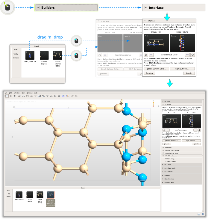
Step 5: The two surfaces do however need to be shifted with respect to each other in the A/B plane. To achieve this, click Shift Surfaces, switch to fractional coordinates, and enter -0.16666666 for both A and B. The preview of the model will update right away in the Builder 3D window:
Tip
You can learn more about the Interface Builder in the Technical Notes on Interface Builder.
Tip
Looking at the article, you will realize that the “Si triangle” in the bottom Si3N4 layer (the layer closest to the interface, atoms 26, 29, 30 (hold the mouse over the atoms to see the numbers in the tooltip) should be ligned with the last Si(111) atom, sitting on the long bond along C, such that they form a tetrahedron. This arrangement means that the Nth atom (atom number 27) which is currently located in the middle of that triangle, at fractional position (2/3, 2/3), should sit right above that Si atom, which has coordinate (1/2, 1/2). Therefore, a surface shift of (-1/6, -1/6) is needed.
Don’t close the “Shift Surfaces” widget yet. As you can see, the two surfaces are also a bit too close to each other. A suitable shift is 0.7 Angstroms (you need to change back to Cartesian coordinates for this one), which gives similar Si-Si and Si-N bond lengths across the interface as in the two respective bulk materials
Close the Shift Surfaces dialog.
Step 6: Add two more layers of Si(111) by clicking
twice for
“Add/Remove layer” under the “First” window. Similarly, for the Si3N4
add at least four layers (it must be an even number of times), depending on
how thick you wish to make the Si3N4.

Final adjustment
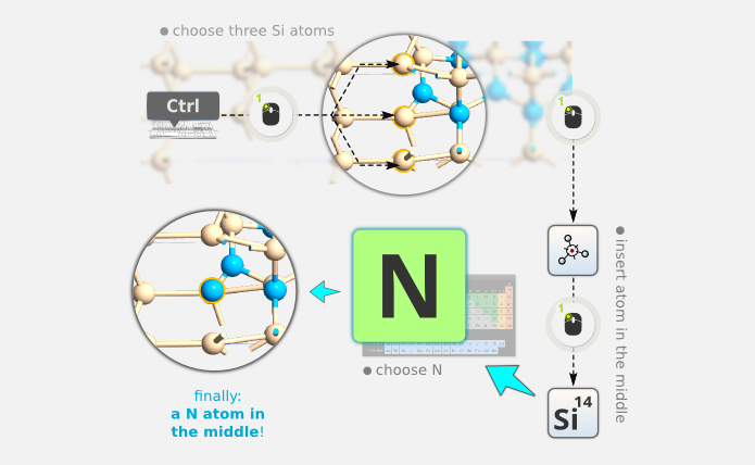
You are not quite done yet. The crucial observation of Yang et al. was that one N atom in the interface needs to be moved, in order for all bonds to be saturated. The atom in question is none other than the one you used for the surface shift, sitting in the middle of the Si triangle (atom number 27).
Step 7: Delete this atom by clicking it to select it, and press Del on the keyboard:

Step 8: Insert a new atom in the middle of the Si triangle in the top layer of the Si (111), by selecting the three atoms (click the first one, then hold down Ctrl when clicking the two others; the atoms in questions are numbers 28, 29, 30), and clicking the “Centroid” plugin
 in the
left-hand side toolbar. The inserted atom has the correct position, but is Si;
change it to N by using the Periodic Table tool
in the
left-hand side toolbar. The inserted atom has the correct position, but is Si;
change it to N by using the Periodic Table tool  :
:
At this point you have a single interface between Si(111) and β-Si3N4(0001), and you may proceed to the next section.
Doubling down: Buried layer model
Tip
One can also take the procedure one step further and create a thin layer of β-Si3N4(0001) embedded in Si(111), i.e. a double interface model. This is fairly easily acieved by mirroring the single interface.
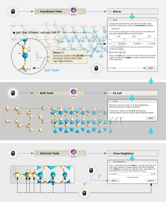
Step 9: Depending on how many Si3N4 layers you added, the size of the current model will be different.
Place the mouse over the last layer in the C direction and make a note of the Z-coordinate of these atoms. In our example here (for Si3N4) the value is 20.5382 Angstroms.
Open . The Z direction is already selected for the normal N, but to get a correctly mirror-symmetric configuration you should place the point P in the last layer. Therefore, enter the value from the previous step into the third box for P, then tick “Copy, and click “Apply”.
Next, adjust the cell by using . Before clicking Apply, make sure only C is ticked, you don’t want to change anything in A or B.
In the reference layer used for the mirror operation, all atoms are now doubled. Therefore, as the final touch, use to select all overlapping atoms and delete them.
Interface as a device model
Irrespective of whether you chose the single or double interface model, the geometry is still represented as a periodic structure. In QuantumATK, you can however compute electronically open systems, as opposed to the periodic models used in other materials science software packages. This means you can compute the properties of a single interface (or two), rather than a periodically repeated stack of different materials.
Open boundary condition calculations are in QuantumATK carried out using so-called device configurations. To convert the current structure into a device:
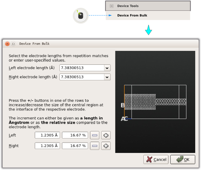
Open .
Since you added a few Si (111) layers, the tool can automatically find the electrode lengths, since there is a repetitive pattern.
Click “OK” to create the device.

Note
As a final note, although it will not be covered here, it should be pointed out that the geometry needs to be optimized, especially the Si atoms in the interface. If you do that, you will see the formation of fully saturated bonds for all Si atoms. To see it in the unrelaxed structure, send the structure to the Viewer, and increase the range for bonds to be plotted to 1.3 Angstroms, and you will see that all Si atoms have 4 bonds.
References