Build a graphene nanoribbon transistor
In this tutorial, you will learn how to build an advanced device using the QuantumATK Builder. We shall consider a nano-scale graphene nanoribbon transistor with a metallic gate separated from the ribbon by a dielectric. This transistor design is inspired by the work presented in [1], where QuantumATK was used to investigate the properties of a similar system.

Fig. 135 The device system considered in this tutorial consists of a z-shaped graphene nanoribbon on top of a dielectric and controlled by a metallic gate. The contour plot illustrates the electrostatic potential along the transport direction.
The device is illustrated in the figure above. It consists of three regions and forms a metal–semiconductor–metal junction. By applying a gate potential across the central region, the system can function as a field effect transistor (FET).
Small nanoribbon transistor
The graphene nanoribbon junction device will be of the zigzag–armchair–zigzag type. You will first build the central region (an armchair nanoribbon) and the two electrodes (zig-zag nanoribbons).You will then proceed to merge together the three components and build the complete junction device.
Central region
Open the  Builder and do the following:
Use the Nanoribbon plugin via to create a graphene nanoribbon.
Tick “passivate dangling bonds with hydrogen atoms”.
Choose a width of 4 atoms.
Choose “armchair edge” as the ribbon chirality.

Use to repeat the ribbon 5 times along the C axis to create the central region.

Electrodes
You are now ready to set up the two electrodes, consisting of two identical zig-zag nanoribbons.
Again, create a ribbon from . This time you should select a 6 atoms wide zigzag edge nanoribbon.
Repeat the bulk configuration 4 times along the C axis.
In order to create two distinct electrodes, make a copy of the newly created zigzag nanoribbon in the Stash.

Merge the three components
Two steps a required:
You first create the z-shaped nanoribbon bulk configuration.
Then turn the bulk configuration into a device configuration used in first principles transport calculations.
Z-shaped nanoribbon structure
You need to connect the armchair nanoribbon (central part) with the two zigzag nanoribbons (electrodes). First, rotate the central part by 30 degrees:
Select the armchair nanoribbon from the Stash.
Use to rotate the central region 30 degree around the x axis.
Go to and fix the cell along the B axis.
Now you can merge the three parts together:
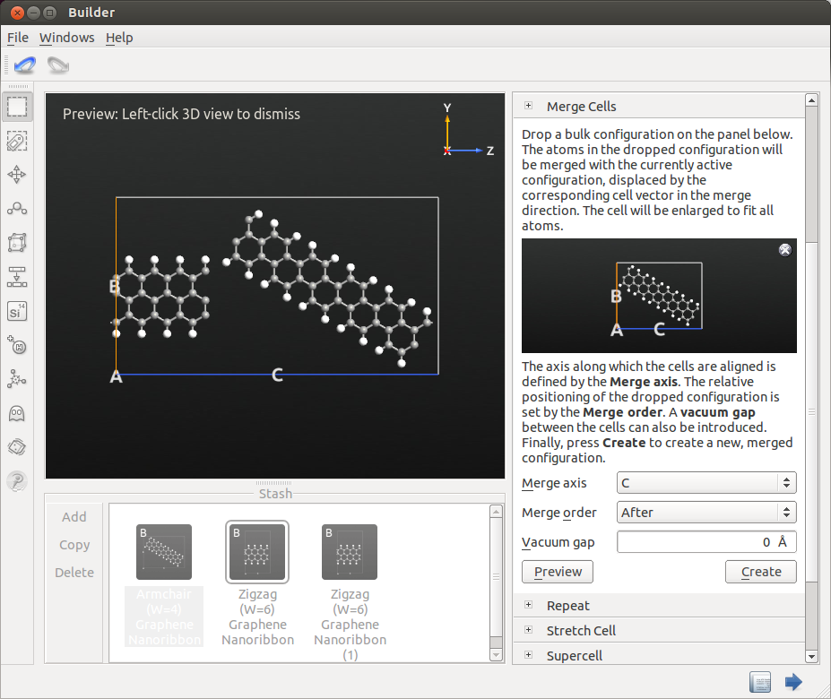
Select the left electrode by double clicking the configuration on the Stash.
Select and drag the central region configuration from the Stash to the small window on the right side as shown below.
Click Create.
Select all the atoms belonging to the central region and activate the
 Move Tool in the tool bar.
Select the lower-left edge atom of the central region as shown below. This atom is now the anchor atom which means that all the other atoms will follow this atom when they are moved.
Be sure that the Snap function is selected then drag your anchor atoms close to the right edge atom of your electrode.
On the Move window you should now be able to see that two atoms are overlapping. Click Fuse to delete one atom for each pair of overlapping atoms.
Close the Move window and delete the extra H between the two carbon atoms.
You now have a perfect junction between the left electrode and the central region. Repeat the procedure outlined above to attach the right electrode to the new configuration, and you will have finished the merge.

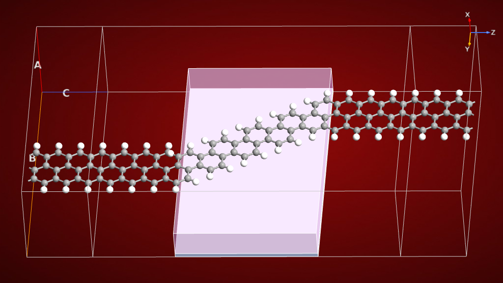
A proper unit cell
Create a proper unit cell and center the configuration in it:
Open , and increase the dimension of the B vector to 27 Å in order to assure sufficient vacuum above and below the configuration.

Use plugin to center the configuration.
The bulk configuration is now finished.
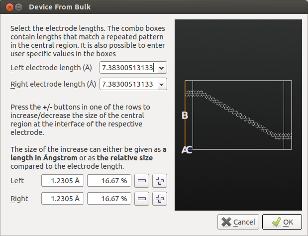
Device from bulk
Transport calculations is a key feature of the QuantumATK platform. The Device Tools plugins help you to construct the device with electrodes and gates.
Highlight the bulk configuration in the Stash, and use the tool to construct the graphene nanoribbon device. The tool will automatically select appropriate electrode lengths.

Note
The required length of the electrode cell depends on the computational model employed. Strictly speaking, the length of the cell in the the C-direction should be longer than the interaction distance of the model. For most models a length of about 7 Å will suffice.
Gate and dielectric
Next, add the metallic gate and the dielectrice separator using the Spatial Regions tool:
Open .
Click
 to insert a new spatial region.
Set the spatial region to be a dielectric region and set the dielectric constant to 4.0.
Use the fractional coordinate fields to define the boundaries of the dielectric region: a:0.05-0.358, b:0-1, c:0.2679-0.7323.
Add a second spatial region, set it to be “metallic” and set the gate potential to -1 V.
Use the fractional coordinate to define the size of the metallic gate: a:0-0.05, b:0-1, c:0.2679-0.7323.

Finally, your device should look like illustrated below.
You can download a script defining the device configuration here: device.py.
Tip
What next? You are now ready to perform some transport calculations! For example, check out the tutorial Graphene nanoribbon device: Electric properties. It shows you how to compute electron transport properties of the gated graphene nanoribbon device, including the electron transmission spectrum, I–V curve, electron thermal transport, and conductance.
You can also proceed to the next section to learn another way to build a nanoribbon transistor.
A longer nanoribbon transistor
There are of course several different ways to build a z-shaped graphene nanoribbon device with the QuantumATK Builder. The approach outlined above constructs the three parts of the device separately and then merge them together. Another possibility is to create the device by “tailoring” an extended graphene sheet. This approach is more flexible, because you can use it to cut out any kind of device based on your needs and imagination.
Use the following this procedure to build a long graphene nanoribbon transistor:
In the Builder, insert a graphene sheet from . Leave the default parameters unchanged and click Build.
Use the plugin to repeat the sheet 1, 6 and 35 times along the A, B and C axes, respectively.

Open the Selection Tool
 by clicking it and choose the Lasso
  from the pop-up list.
Use the Lasso to select the regions of atoms you want to cut out, as shown below.


Tip
You can also use the plugin. You will find this tool very handy in case of complicated but geometrically regular shapes. Click the How-To button for more informations about how to use and combine expressions.
To select the atoms that do not belong to the graphene device, use the two following expressions:
(y > 47) or (y > -0.577*z+52 and 7.39 < z and z < 77.5216) or (y > 6.40 and z > 77.5216)
(y < 1) or (y < -0.577*z+46 and 8.65 < z and z < 77.5216) or (y < 41.91 and z < 8.62)
The first expression selects the atoms to delete in the upper part of the device, while the second expression selects the atoms to delete in the lower part.
Whatever method you choose to cut out the z-shaped device, you should now have a nice z-shaped ribbon. Add a bit of vacuum along the B direction:
Open and increase the B vector dimension to 65 Å. Make sure to keep the Cartesian coordinates fixed in this step.
Use the tool to center the configuration along the B vector.

Next, use the tool to create the device configuration. The default electrode lengths are fine.
The graphene nanoribbon needs to be hydrogen terminated at the edges. Use the Passivate
 tool to saturate all bonds by hydrogen atoms.
Next, you should add the metallic gate and dielectric spacer. Open the plugin and add two regions:
Metallic, -1 Volt, fractional coordinates: a:0-0.05, b:0-1, c:0.08-0.92
Dielectric, 4, fractional coordinates: a:0.05-0.045, b:0-1, c:0.08-0.92
You have now created a long z-shaped graphene nanoribbon device on top of a dielectric and controlled by a metallic gate.

Tip
What next? The transistor you have just built is used in the second part of the tutorial Graphene nanoribbon device: Electric properties. Go directly to the relevant section by following this link: Comparison to results for a longer device.