Effective band structure of random alloy InGaAs
Version: 2015.1
Random alloys are becoming technologically important materials. For example, SiGe is one of the best known thermoelectric materials, and InGaAs is a prime candidate to substitute or complement silicon in future CMOS devices. Simulations of both thermoelectric elements as well as transistor devices often refer to band structure parameters such as band gaps and effective masses.
In this tutorial, you will lean how to setup the structure of a random alloy and calculate the so-called effective bandstructure. The tutorial will focus on In0.53Ga0.47As and calculations will be performed with DFT using the TB09-MGGA exchange-correlation functional, in order to obtain accurate band gaps.

Note
In a normal band structure, each band is a line with zero width/broadening in both the E- and k-directions: Bloch’s theorem applies and the wavenumber k is a good quantum number. In a disordered alloy, Bloch’s theorem strictly does not apply, and one cannot a priory know if k is still a good quantum number or if the whole concept of a band structure is well defined.
In QuantumATK 2015 it is possible to calculate “effective band structures” of random alloys, following the method described in Refs. [1][2][3]. The purpose is to investigate whether or not the random alloy band structure is well defined, and if it is reasonable to extract band parameters.
Methodology
In the calculation of effective band structures, one considers a large super-cell containing many atoms. Here we consider a 3x3x3 repetition of the primitive FCC unit cell with 64 atoms. We model In0.53Ga0.47As as InAs with some of the indium atoms replaced at random with gallium atoms. The In/Ga ratio is kept fixed at 0.53/0.47 in all calculations.
From the band structure of the super-cell containing more than 500 electronic bands, one can “unfold” the band structure such that it only contains bands corresponding to the primitive cell. In the unfolding procedure, one calculates a spectral weight \(\mid \langle e^{ i \bf{k} \cdot \bf{r}} \mid \psi_{j,K} \rangle \mid\), where \(\mid \psi_{j,K} \rangle\) is an eigenstate of the super-cell at k-point \(K\). If the super-cell is simply a copy of a simple unit cell (e.g. a super-cell of InAs), the spectral weights will either be 0 or 1, and the band unfolding can be done explicitly. However, in the case of a disordered alloy, such as In0.53Ga0.47As, the band weights can be any real number between 0 and 1.
Band structures of InAs
You will first calculate the normal band structure of a InAs, using the primitive (1x1x1) unit cell. Then a 3x3x3 InAs configuration is created, and you will show that the effective band structure of this repeated super-cell reproduces that of the primitive cell.
1x1x1 InAs
Open the Builder
 and go through the following steps:
Use the tool to create the InAs bulk configuration.
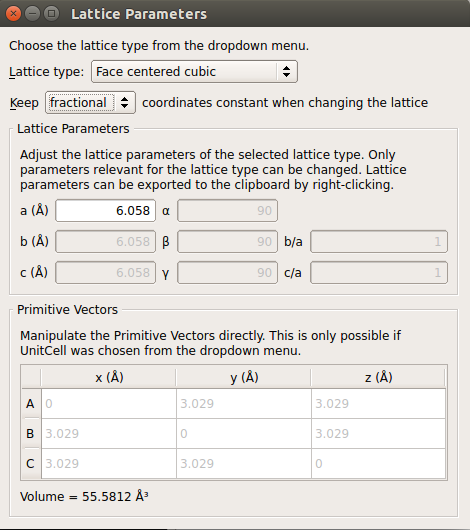
Use the tool to change the lattice constant to the room temperature value:
Choose keep fractional;
Type in a = 6.058 Å.
Click OK and send the configuration to the Scripter
 .
.
In the Scripter add a
 New Calculator block. Then open and edit it:
Select the ATK-DFT calculator.
Use MGGA for exchange-correlation potential.
Set up a 9x9x9 grid for k-point sampling.
Use a SingleZetaPolarized basis set to speed up calculations.

Next, add an
 block.
Open it and set the Brillouin zone route to “L, G, X”.
block.
Open it and set the Brillouin zone route to “L, G, X”.Change the Default output file name to
InAs_1x1x1.hdf5.Transfer the script to the Editor
 in order to specify the TB09-MGGA c-parameter. Locate the line
exchange_correlation = MGGA.TB09LDA
and change it to
exchange_correlation = MGGA.TB09LDA(c=0.91)
Run the calculation using the Job Manager
 or
in a Terminal. It takes about eight minutes to complete the simulation.
or
in a Terminal. It takes about eight minutes to complete the simulation.
Note
You can learn more about the TB09-MGGA exchange-correlation potential and the TB09-MGGA c-parameter from the tutorial Meta-GGA and 2D confined InAs.
3x3x3 InAs
Back in the Builder
, repeat the 1x1x1 InAs configuration
3 times in each direction using the tool.Send this configuration to the Scripter
and repeat
the procedure outlined above to set up a script, buth with the following changes:The k-point sampling in the calculator should be 3x3x3.
The default output file name should be
InAs_3x3x3.hdf5.
Use again the Editor
to explicitly set the TB09-MGGA c-parameter,
and run the calculation.
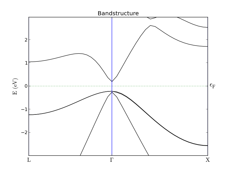
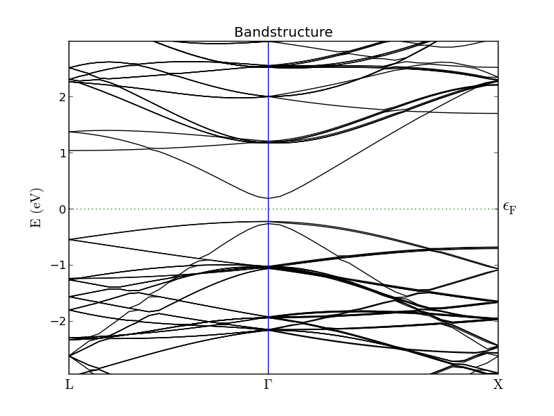
Results
The band structures for the 1x1x1 (left) and 3x3x3 (right) InAs configurations are shown below. The 3x3x3 band structure is folded at the zone boundaries, which makes it hard to locate the valleys corresponding to the X- and L-valley minima of the 1x1x1 configuration.
Effective band structure of 3x3x3 InAs
Open a new Scripter window, and follow these steps:
Add the
 Analysis from File block, open it,
and select the existing HDF5 file
Analysis from File block, open it,
and select the existing HDF5 file InAs_3x3x3.hdf5.Add also the
block.
It will be crossed over, indicating that the block needs further editing.
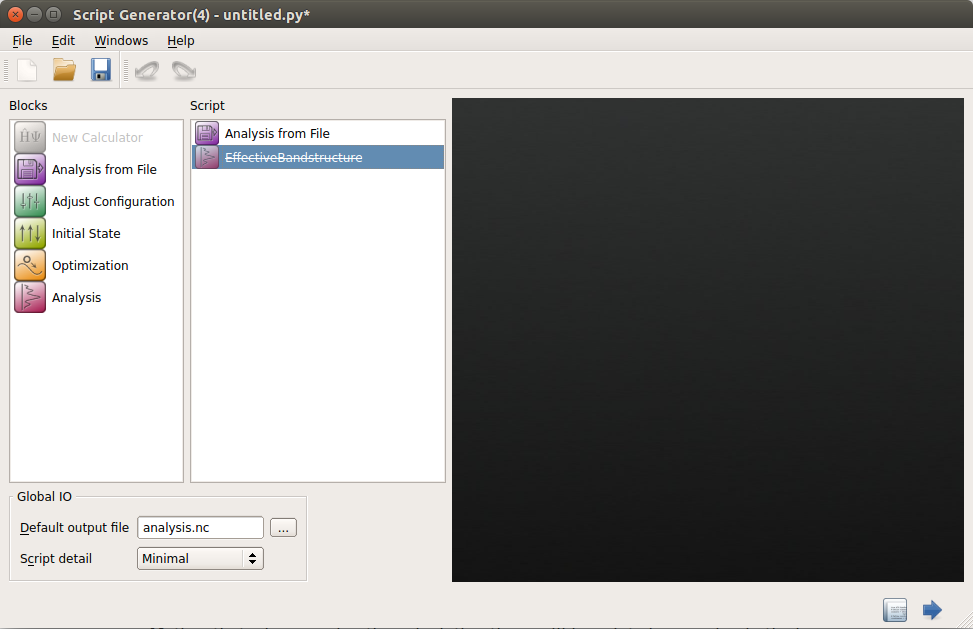
Open the EffectiveBandstructure block and start editing it.
Select a 1x1x1 InAs configuration, either from the Builder or from the LabFloor, and drag it to the black area named “Primitive configuration”.
Apply the following settings:
Points pr. segment: 101
Brillouin zone route: L, G, X
E0: -2.0 eV
E1: 2.75 eV
Points: 501
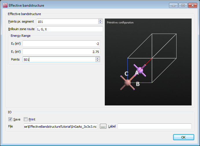
The script is now done, so save it and run the calculation. It takes about three minutes to complete on a laptop.
Note
When running the calculation the folllowing warning will appear in the log file:
Warning: The calculation did not converge to the requested tolerance!
This is perfectly OK. A single SCF iteration is executed to obtain the basis functions in the primitive cell, which are used in the effective band structure calculation.
The EffectiveBandstructure object will now have appeared on the LabFloor. It looks like this:

Select the object and use the Effective Bandstructure Analyzer plugin to visualize it. Compare the figure (shown below) with the normal band structure plot of the 1x1x1 InAs shown above.
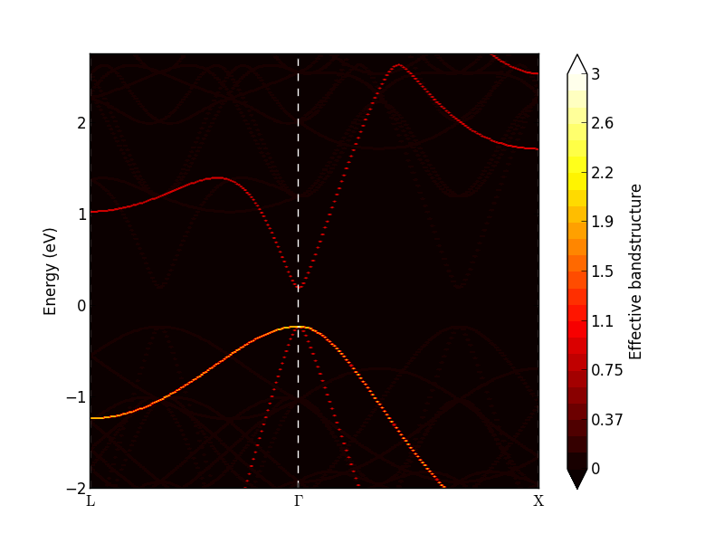
The analyzer shows a band density map of the k,E(k) plane. Each band will add a weight between 0 and 1 to the band density. At the \(\Gamma\)-point there are three degenerate valence bands, and the band density becomes 3 (bright yellow in the figure above). The conduction band has a weight of 1.
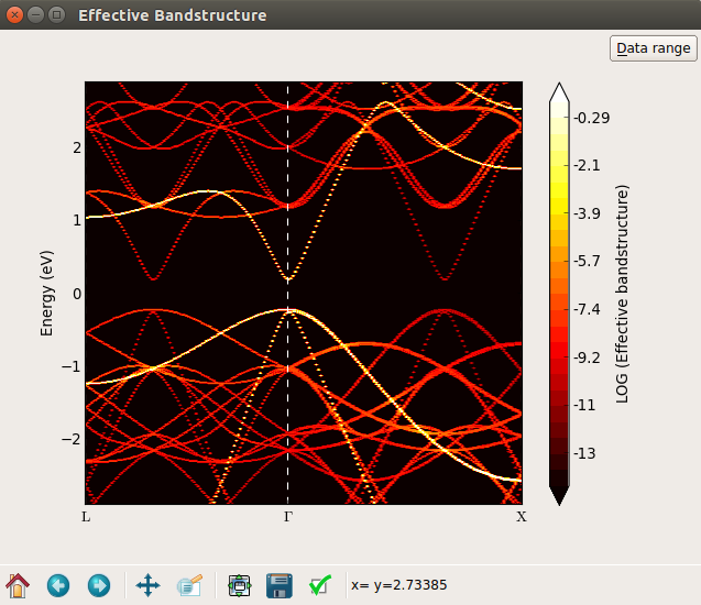
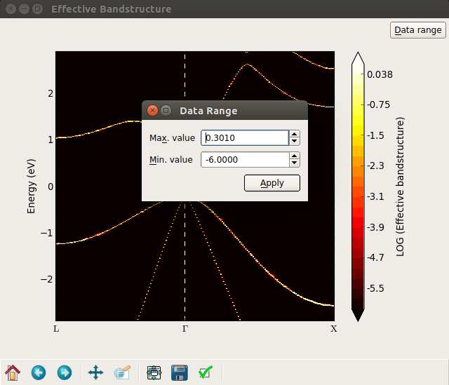
In order to see all the bands with a weight close to 0, you can plot the band density on a logarithmic scale. Right-mouse click on the plot and select Log scale in the bottom of the menu, and the plot is shown as the left figure below. A lot of bands appear in red color. By inspecting the colorbar you notice that these bands have weights around 10-9, which is essentially just numerical noise. Try to adjust the “Data range” (upper right corner) and set the minimum value to -6. The “noise bands” now disappear, as shown at the right figure below.
Important
So far, you have seen that the effective bandstructure works, and give what we expect: The effective band structure of the 3x3x3 repeated InAs is the same as the normal bandstructure of the simple 1x1x1 InAs.
In the next section you will learn how to setup a random InGaAs alloy – a system where the normal bandstructure cannot be calculated for a simple 1x1x1 configuration, and where it is not a priori obvious if the whole concept of a band structure is well-defined or not.
In0.53Ga0.47As random alloy
You will now set up a In0.53Ga0.47As random alloy structure and calculate the effective bandstructure. We shall also consider the sample averaged effective band structure, and analyze the consequences of finite band broadening.
Random alloy
Open the Builder to create the alloy configuration:
Add a new InAs configuration, and change the lattice constant to 5.8687 Å, which is the experimental value for In0.53Ga0.47As.
Right-click the new Stash item and copy it (you will need the copy later on for calculating the effective bandstructure).
Repeat the InAs configuration 3 times in each direction.
Next, select all the indium atoms by using the tool, and open the plugin. Apply the following settings:
Algorithm: Fixed fraction
New element: Ga
Percentage: 47%
Then click Create.
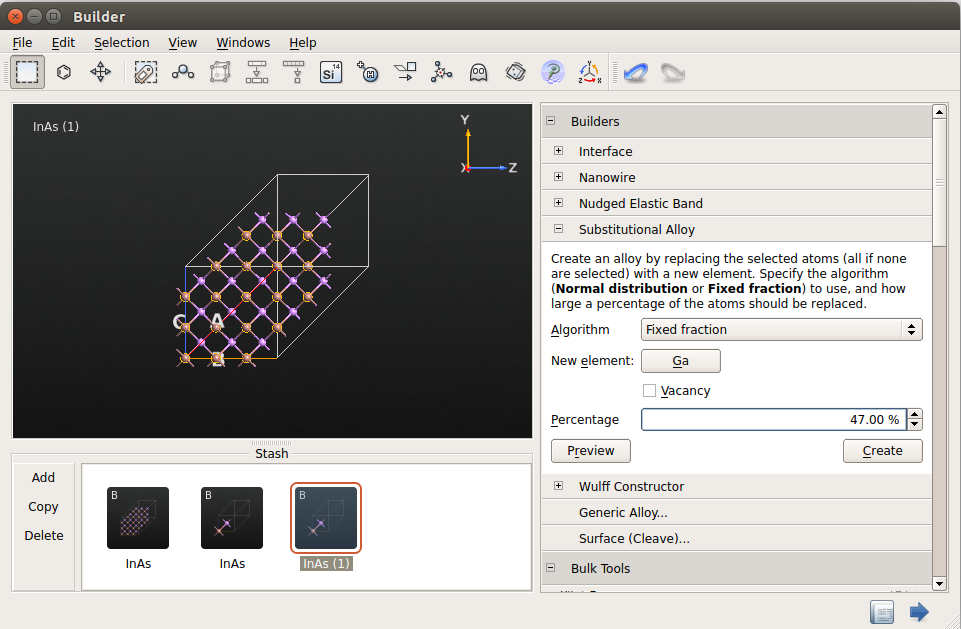
In the new configuration, approximately 47% of the indium atoms have been
substituted with gallium atoms in a random way. Transfer this In0.53Ga0.47As
random alloy configuration to the Script Generator .
Effective band structure calculation
Add a
New Calculator block with the same settings as used for InAs:MGGA exchange correlation.
3x3x3 k-point sampling.
SingleZetaPolarized basis set.
Add the
block,
and open it for editing.Drag-and-drop the copied 1x1x1 InAs configuration with the 5.8687 Å lattice constant from the Builder onto the black area.
Apply these settings:
Points pr. segment: 101
Brillouin zone route: L, G, X
E0: -2 eV
E1: 2.75 eV
Points: 501
Transfer the script to the Editor
and add the TB09-MGGA c-parameter.
For In0.53Ga0.47As with a SingleZetaPolarized basis set, you should use c=1.01 to get
approximately the experimental band gap of 0.74 eV.Run the job using Job Manager
or in a Terminal.
It takes about 10 minutes to complete the job.
Results
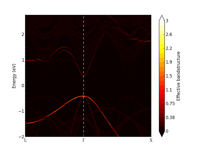
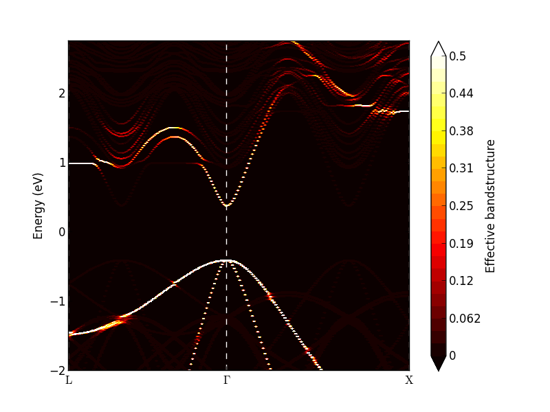
Investigate the calculated effective band structure using the Effective Bandstructure Analyzer. It should be similar to the figure on the left below. The bands are no longer weighted at either 0 or 1, but with a value in between. In particular around the L- and X-point conduction band minima, there are clear deviations from the simple band structure seen for InAs. Try to adjust the data range and set the maximum value to 0.5. Then some of the bands become more visible, as shown below on the right. Near the \(\Gamma\)-point, both the valence band and conduction bands are well-defined, and the effect of the random disorder seems to be rather limited.
Note
The resulting effective bandstructure is not necessarily exactly the same as in the figure above due to the random alloy generation.
Sample averaged effective band structure
A quantitatively more reliable effective band structure should be obtained by repeating the above procedure a number of times to create different random configurations. Some python scripting can help to finish the task elegantly and efficiently.
Download the Python script ingaas_ebs.py, which creates a number of random In0.53Ga0.47As alloys
and performs the effective band structure calculation for each of them. You can then
average over the results. The default number of generated alloys (number_of_runs) is 10.
You will get even better results by increasing that number.
Run the script, and observe the EffectiveBandstructure objects appear
in the file InGaAs_3x3x3.hdf5 on the LabFloor.
Mark all the generated data objects and click the Effective Bandstructure Analyzer.
The analyzer will now show the average of all the effective band structure densities.
Try to adjust the colours by changing the data range and maximum value:
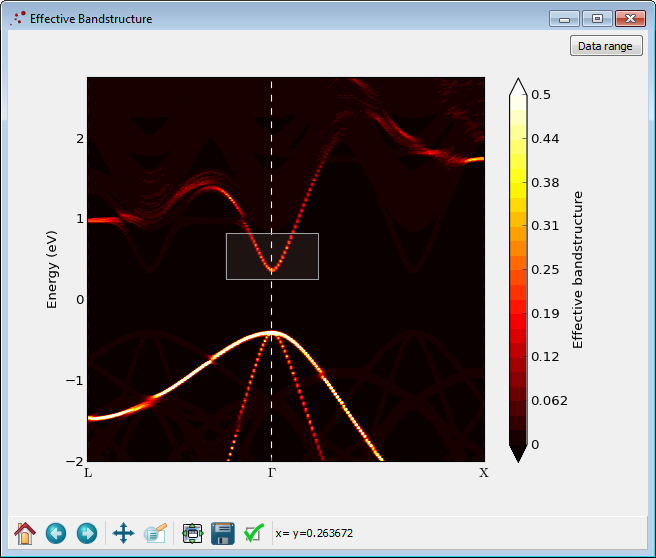
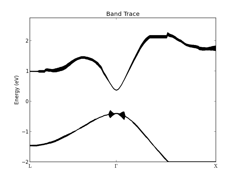
It is possible to trace the most significant bands with the heighest weight: Draw a box with the mouse like shown in the figure above. A progress bar will appear in the bottom of the window signalling that the effective band structure data is being analyzed for band tracing. After a little while a new window will appear, like the one shown below. The figure shows the traced bands plotted with a finite with. The center of the line is identified as a band. It can be exported to a text file by right-clicking on the figure and choosing Export data.

Tip
The band is calculated in the following way:
For each k, the band density is first smoothed by performing a convolution with a Lorentzian function (the broadening in energy is 0.2 eV).
The peaks of this smoothed band density is found.
A band is formed by selecting the peak energies closest to the peak energy found at the previous k-point (or, for the first k-point, closest to the center of the box you draw).
Proceed to the next k-point and repeat the process.
The width is calculated as the second moment of the raw data (i.e. not smoothed) in an interval of -0.15–0.15 eV around the peak energy. The maximum width is thus 0.3 eV. Note that if two or more bands are close to each other, the calculated width will be slightly wrong, since the density from the other bands will contribute to the width. Try to draw a box around the highest valence band. The Band Trace figure will be quickly updated to appear like the figure below. Close to the \(\Gamma\)-point the senond-highest valence band erroneously contribute to the width of the first one.
Finite broadening
Contrary to a normal band structure, the effective bands will have a finite broadening. If the broadening is small, the band structure is well-defined; if the broadening is large, the concept of bands is no longer valid. The average effective band structure of an In0.53Ga0.47As random alloy, as shown in the figure above, is well-defined close to the \(\Gamma\)-point. However, the conduction band is not well-defined around the L- and X-valley minima, where the bands have a finite broadening of \(w \approx\) 0.06 eV.
The well-defined effective band structure around the \(\Gamma\)-point can be understood in terms of the long wavelength present there. The local random variations are not “seen” by a long wavelength electron. On the contrary, at the X and L points, the wave functions vary on the atomic scale, and are affected by the disorder.
Analysis and consequences of finite band broadening
One can interpret the finite band broadening in terms of a life-time \(\tau = \hbar / w =\) 11 fs. Together with an approximate longitudinal effective mass \(m_l\)=1.5 \(m_e\) and transverse effective mass \(m_t\)=0.2 \(m_e\), both obtained from virtual crystal approximation (VCA) calculations, we can estimate the effective mean free path (MFP) as:
where the band velocity \(v_k = 1/\hbar \cdot \partial E(k)/\partial k\). Assuming a parabolic band \(E(k) = \hbar^2 k^2/2m\) around the valley minima, the mean free path as a function of energy, relative to the X- or L-valley minimum, is then:
At the valley minima, the mean free path vanishes, and at a constant energy surface
of 0.01 eV above the X- or L-valley minima we obtain estimated mean free paths
of 1.5 nm and 0.5 nm in the transverse and longitudinal directions, respectively.
Clearly, the random disorder will be a limiting factor for transport in these valleys.
The MFP vs. energy can be plotted with the python script mean_free_path.py.
Final comments
For scientific use we recommend to use even larger super-cells, e.g. 4x4x4 or even larger, which will be more like a real random alloy. The relatively small 3x3x3 cell used in this tutorial was chosen to make the calculations relatively fast. The small cell size might affect the results in a quantitive manner, but we do expect the main conclusions to remain unchanged.
Since the effective band structure close to the \(\Gamma\)-point has a narrow broadening, it is reasonable to assume that Bloch’s theorem applies here and that the random disorder has a small effect on the transport properties. In this case, more efficient studies of the band structure of random alloys can be performed with the virtual crystal approximation as explained in the tutorial Virtual Crystal Approximation for InGaAs random alloy simulations.